Novel Elliptic-function Low-pass Filter (LPF)
| ✅ Paper Type: Free Essay | ✅ Subject: Computer Science |
| ✅ Wordcount: 2743 words | ✅ Published: 07 Aug 2018 |
Performance of microstrip low pass filter with stub loaded Electromagnetic Band Gap ground plane
- Mariselvam V, Raju S
Abstract
A novel elliptic-function low-pass filter (LPF) is Presented, which consists of a Electromagnetic band gap on the ground plane. The Electromagnetic band gap provides the required wideband attenuation in stop band, while the slot provides steep transition from pass band to stop band. A 5.4 GHz five-pole LPF is developed and experimental results show that it has a sharp cutoff frequency response. The measured pass band insertion-loss is below 0.4 dB, and the rejection band over 15 dB is from 5.425 GHz to 8.25 GHz, Which increases from 2.95 GHz.
Keywords: Defected ground structure (DGS), elliptic-function filter, low-pass filter (LPF).
1. INTRODUCTION
Recently, defected ground structure (DGS) has become one of the most interesting areas of research in microwave and millimeter wave Applications [1]. It could be widely used in microwave circuit design such as power divider, power amplifier and especially in filter design [1–9]. Low pass filters (LPF) design require that both in-band and out-band performances should be: low loss, high selectivity, high rejection, and wide spurious free frequency ranges. Many novel types of microstrip filters have been proposed and designed. Periodic or non-periodic DGS are realized by etching a slot in the backside metallic ground plane. The etched slot disturbs effectively the current distribution in the ground plane of microstrip line and the results in resonant characteristics [2, 3].
IT is well known that typical properties of low-pass filters (LPFs) can be obtained by adding periodic structures to transmission lines. The representative periodic structures for planar transmission lines and/or microwave circuits are photonic band gap (PBG) and defected ground structure (DGS) [4, 5]. The PBG has been known as a popular periodic structure for planar transmission lines. However, drawbacks of PBGs have been also discussed as follows.
1) A large area is needed because a number of periodic patterns should be adopted.
2) It is obscure to define the unit element, and difficult to extract the equivalent-circuit elements for the PBG unit element.
3) Therefore, it is very restricted to extend its practical application to microwave circuits. To the contrary, one can easily define the unit element of the DGS and model the equivalent circuit.
In addition, since only a few DGS elements show the typical properties of periodic structures, the resultant circuit size becomes relatively small. Furthermore, the structure of the DGS is simple and it is easy to design the DGS pattern. For these reasons, since [4] has introduced the structure and called it a DGS for the first time, the DGS has been extensively applied to design microwave circuits such as filters, power dividers, couplers, amplifiers, oscillators, and so on [1], [6]–[12].
There is much previous research about the characteristics of LPFs having periodic structures on microstrip or Coplanar waveguide (CPW) transmission lines [13]–[16]
However most of them are not analytical because they mainly depend on electromagnetic (EM) simulations to design LPFs and predict circuit performances. To the contrary, in the design of LPFs using DGSs including this study, all design steps are based on theories and reasonable explanations as follows.
- The equivalent-circuit elements of the DGS is extracted and used for replacing the series inductances in the LPF Prototype circuit.
- The LPF is composed of the extracted equivalent lumped Elements, thus, it is an ideal LPF, is designed, and is compared to the realized LPF using the DGS practically.
Two methods to design a three-pole LPF using the DGS has been proposed in [1] and [6]. In these papers, the sizes of two DGS patterns in the LPF were exactly the same because two inductances in the three-pole “L1 (series) – C2 (shunt) – L3 (series)” prototype LPF are identical. In [6], discontinuity elements such as tee- or cross-junctions were adopted to connect open stubs to realize the shunt capacitance. However, in the three-pole LPF proposed in [1], there are no junction elements, thin transmission lines for high impedance, or open stubs. In addition, the width of the transmission-line elements in the LPF has been remarkably broadened. Thus, advantages such as compact design and error-robust realization fabricating the layout have been obtained. However, in order to design -stage LPFs using the DGS, e.g., a five-stage like “L1 (series) – C2 (shunt) – L3 (series) – C4 (shunt) – L5 (series),” two different dimensions of the DGS have to be adopted because L3 is not equal to L1=L5, although. In order to select the proper dimension of the DGS for L3 careful consideration based on filter theories, extracted equivalent- circuit elements of various DGS dimensions, and some related topics of transmission lines should be taken. The size of the DGS for L3 is determined by accurate curve-fitting results for equivalent-circuit elements to correspond exactly to the required inductance. In addition, the length of transmission-line elements between DGS patterns is determined through the consideration for the equivalent capacitance and additional parasitic inductance, as well as the required shunt capacitances in the prototype LPF. Therefore, a design of a five-pole DGS-LPF requires many more complex steps than the previous three-pole DGS-LPF shown in [1] and [6]. Thus, the goal of this paper is to propose a new technique to design an -pole LPF having (“DGS-LPF”), and to generalize the previous design method for N>5 using different sizes of DGS patterns. For this purpose, modeling for the equivalent circuit of the DGS, a curve fitting for determining the required different sizes of the

Fig.1 Top view of the Microstrip line with a DGS pattern and its dimensions in mm

Fig.1a. Bottom view of the Microstrip line with a DGS pattern and its dimensions in mm
DGS that reflects the inductance values in the prototype LPF and a practical design example will be successively discussed.
In order to show the validity of the proposed method, a five pole DGS-LPF, as an example, is designed and measured in this paper. The five-pole DGS-LPF has a much wider microstrip line than conventional microstrip LPFs, and does not include high-impedance lines, which have been essentially required in conventional design. The series inductances in the prototype LPF are realized by DGSs, while the shunt capacitances are realized by the widely compensated transmission line. Therefore, no discontinuity elements such as tee- or cross-junction for connecting open stubs are required because there are no stubs in the DGS-LPF.
2. DGS PATTERN AND MODELING FOR THE EQUIVALENT CIRCUIT
Fig. 1and 1a shows a microstrip line having a dumb-bell DGS and its -parameters from an EM simulation. Two elliptical defected areas and one connecting slot correspond to the equivalently added inductance (L) and capacitance(C), respectively. Accordingly, a resonance occurs at a certain frequency because of the parallel L–C circuit. Inversely, it is intuitively known that the equivalent circuit includes a pair of parallel inductor– capacitor from the resonant phenomenon in the -parameter. This means the microstrip line having the DGS does not have all-pass characteristics, but restricted pass band properties.

Fig.2. Equivalent circuit of the microstrip line with unit DGS using ADS
In addition, slow-wave characteristics are observed due to the added– components of the DGS [3], [5], [9]. The defected areas can be realized by not only ellipse, but also other geometries such as triangle, circle, hexagon, octagon, spiral, and so on. It is very clear that the resonant frequency (wo) of the DGS and 3-dB cutoff frequency (wc 3dB) exist as shown in Fig. 1.The equivalent – circuit of the DGS can be extracted because this kind of electrical characteristic is observed from a typical L –C parallel resonant circuit.
The equivalent circuit of the DGS and one-pole Butterworth prototype of the LPF are presented the DGS in Fig. 2. The equivalent L– C elements are calculated by (1–3) because two reactance values of Fig. 2(a) must be equal at wc 3dB as follows
XLc= (1)
(1)
XL = ω’Zo g1 (2)
XLc | ω= ωc, (3)
Where w'(=1), g1 (=2) and Zo (=50Ω) are the normalized 3-dB cutoff frequency, element value of one-pole Butterworth prototype LPF, and port impedance, respectively, and wo = (1/√ Lk1Ck1). The calculated L2and c2 of the DGS shown in Fig. 2 are 3.2 nH and 0.8194 pF, respectively. Fig. 3 shows an excellent agreement between the previous -parameters shown in Fig. 1 and the new ones calculated using Lk1and ck1. Advanced Design System (ADS), a circuit simulator from Agilent Technologies, has been used for the calculation. This agreement means that the modeling technique is valid in extracting the equivalent-circuit elements. It should be noted that this is one of the great advantages of DGS because it is possible to define the unit element of the DGS and to establish the equivalent circuit of it, while the conventional Planar transmission lines with a periodic structure such as a PBG have difficulty in defining the unit element and to extract the modeled circuit element.
2.1 DESIGN OF THE FIVE POLE LOWPASS FILTER
A. Prototype LPF and Adoption of DGS
The method to design a five-pole LPF using the DGS is discussed here. Fig. 3 depicts the prototype circuit of a five-pole LPF. Here gi (i=0, 1, 2, 3, 4, 5, 6), represent the normalized element values of a Chebyshev prototype LPF for the given ripple [17]. According to the design theory of filters, in order to transform the prototype LPF to the LPF composed of lumped elements, the values of L1,C2,L3,C4 and L5can be determined owing to the impedance and
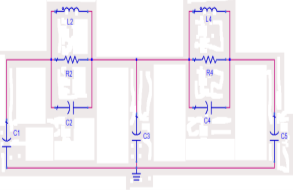
Fig.3. Five-pole Chebyshev prototype LPF with Elliptic DGS

Fig.3a. Equality of a series inductor to an LC parallel circuit
frequency scaling rules expressed in (4)–(6). Here, ωc means the Cutoff frequency of the LPF
L1 = =
=  = L4 (4)
L3 = (5)
(5)
C2 =
 = C4 (6)

Fig.4. Performance of the designed five pole LPF using ADS

Fig.5. Performance of the designed five pole LPF using CST
2.2 PERFORMANCE OF THE DESIGNED DGS-LPF
FIG. 6 shows the measured S-parameters of the designed DGS-LPF, as compared with the theoretical performance (circuit simulation) and the EM simulation by CST-MWS. As shown, the measurement result agrees with the EM simulation very well. The designed elliptical function DGS-LPF exhibits a much shaper transition knee than the Chebyshev one reported in [5]. Its transition bandwidth from 1 to 20 dB attenuation is only 0.45 GHz. The measured pass band insertion loss is less than 0.3 dB. The stop bandwidth corresponding to 15dB rejection is from 2.95 to 8.25 GHz. The total length of the designed DGS-LPF is 17 mm, and compared with the LPF reported in [5], it is reduced about 40.88% and compared with the LPF reported in [6] it is reduced about 14.66%.

Fig.6. Measured result of the designed five pole LPF using Agilent Network analyzer N5230A
3. PERFORMANCE OF THE PROPOSED DGS LOWPASS FILTER


Fig.7. Top view of the Microstrip line and its dimensions in mm

Fig.7a. Bottom view of the Microstrip line and its dimensions in mm
The proposed five-pole DGS-LPF has a much wider microstrip line than conventional microstrip LPFs, and does not include high-impedance lines, which have been essentially required in conventional design. The series inductances in the prototype LPF are realized by DGSs, while the shunt capacitances are realized by the widely compensated transmission line. A stub like elements which gives a inductance effect is introduced in the proposed DGS-LPF.
DGS combined with microstrip line causes a resonant character of the structure transmission with a resonant frequency controllable by changing the shape and size of the slot. There is a huge evolution in terms of defected shapes: dumbbell, periodic, fractal, circular, spiral, and L shaped [12–14]. In this paper, a novel elliptic shape DGS is proposed for the LPF design. The use of elliptic shape DGS will be shown to give sharp cut off frequency response as well as a good performance in the pass band. The analysis of the dimension parameters with different dimension parameters was demonstrated as a design guide. The equivalent circuit (EC) has been extracted to characterize the proposed low-pass filter. The equivalent circuit model agrees with the field simulation results. The theoretical and measured results are presented with good agreement for LPF. The total length of the designed DGS-LPF is 15 mm, and compared with the LPF reported in [5], it is reduced about 60% and compared with the LPF reported in [6] it is reduced about 29%, the pass band increases up to 5.425 GHz from 2.95 GHz and the stop bandwidth corresponding to 15dB rejection is from 5.425 GHz which is suitable for WLAN application
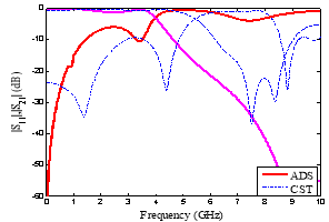
Fig.8. Comparison Performance of the designed five pole LPF

Fig.9. Equivalent circuit of the microstrip line with unit DGS using ADS

Fig.10. Measured result of the proposed five pole LPF using Agilent Network analyzer N5230A
|
Elliptic |
Circular |
Dumbbell |
|
|
S21 (dB) |
-0.58 |
-0.69 |
-0.48635 |
|
S11(dB) |
-36.69 |
-33.5 |
-35.129 |
Tab 1: Performance of the five pole LPF using CST
|
Elliptic |
Circular |
Dumbbell |
|
|
a |
3.35 |
2.5 |
3.35 |
|
b |
2.75 |
2.5 |
3.35 |
|
c |
1.5 |
1.5 |
1.5 |
|
d |
2.4 |
2.4 |
2.4 |
Tab 2: Dimensions of the proposed DGS designs
|
Prototype elements |
Designed LPF |
Proposed LPF |
|
L2 |
3.2nH |
0.454nH |
|
L4 |
3.8nH |
0.38nH |
|
C2 |
0.894pF |
0.71pF |
|
C4 |
0.516pF |
0.43pF |
|
C1 |
0.7704pF |
0.264pF |
|
C3 |
1.9054pF |
1.4pF |
|
C5 |
1.1271pF |
1.1271pF |
|
L5 |
– |
3.38nH |
|
L6 |
– |
3.13nH |
Tab3. Prototype elements of the five pole elliptic function LPF

Fig.11. Top view of the prototype

Fig.11a. Bottom view of the prototype
4. CONCLUSION
This letter has presented a new LPF to obtain elliptic-function response using Dumbbell shaped DGS. The designed LPF exhibits sharp cutoff frequency response, low insertion loss, and excellent stop band performance. The proposed design procedure can be extended to arbitrary -stage LPF. In addition, its physical structure is only composed of defect and microstrip line, so it is easy to fabricate. Since this design is simple, analytical, and does not require any optimization process, this kind of equivalent circuit model of DGS and its design technology may be further applied to various microwave circuits such as low-noise amplifiers, diplexers, mixers, and so on.
References
- SERGIO PALMA PACHECO, JIANEI WANG, JONG- GWAN YOOK, AND LINDA P. B. KATEHI, “ Micromachined Filters on Synthesized Substrates Rhonda Franklin Drayton,” IEEE Trans. Microwave Theory Tech, 2001, Vol. 49, No. 2.
- SYSTEMS PIERRE BLONDY, ANDREW R. BROWN, “Low-Loss Micro machined Filters for Millimeter-Wave Communication”,1998 IEEE vol.38, pp 22-23.
- C. Y. CHI AND G. M. REBEIZ “Conductor loss limited stripline resonator and filters,” IEEE Trans. Microwave Theory Tech., 1996, vol. 44, pp.626–629.
- S. V. ROBERTSON, L. P. B. KATEHI, AND G. M. REBEIZ, “Micromachined self-packaged W-Band bandpass filters,” in IEEE MTT-S Symp. Dig., 1995, pp. 1543–1546.
- J. S. LIM, C. S. KIM, D. AHN, Y. C. JEONG, AND S. NAM, “ Design of low-pass filters using defected ground structure,” IEEE Trans. Microw.Theory Tech., 2005, vol. 53, no. 8, pp. 2539–2545.
- JINPING YANG AND WEN WU “Compact Elliptic-Function Low-Pass Filter Using Defected Ground Structure” IEEE Microwave and Wireless components letters, 2008, Vol. 18, No. 9.
- GAËTAN PRIGENT, ERIC RIUS, FRANÇOIS LE PENNEC, SANDRICK LE MAGUER, CÉDRIC QUENDO, GONZAGUE SIX, AND HENRI HAPPY, “Design of Narrow-Band DBR Planar Filters in Si–BCB Technology For Millimeter-Wave Applications ” 2009 IEEE xplor.Vol.13.
- R. F. DRAYTON, S. PACHECO, J.-G. YOOK, AND L. KATEHI, “Micromachined filters on synthesized substrates,” in IEEE MTT-S Int. Microwave Symp. Dig., 1998, pp. 1185–1188.
- S. DEEPAK RAM PRASATH, A. THENMOZHI, P. SRINIVASABHARATHWAJ, S.RAJU, AND V.ABHAIKUMAR “A Novel Miniaturized Filter on Micromachined Multilayered Substrates” IETE 2008, Vol.54, No.2.
- RHONDA FRANKLIN DRAYTON, SERGIO PALMA PACHECO, JIANEI WANG, JONG-GWAN YOOK, , AND LINDA P. B. KATEHI “ Micro machined Filters on Synthesized Substrates”, IEEE Trans. Microwave Theory Tech.,2001, vol.49, no. 2.
- S.RIKI BANERJEE AND RHONDA FRANKLIN DRAYTON, “ Circuit Models for Constant Impedance Micro machined Lines on Dielectric Transitions”, IEEE Trans. Microwave Theory Tech.,2004, vol. 52, no. 1, pp. 105-111.
- B.F. ZONG, G. M. WANG, H. Y. ZENG, Y. W. WANG. “Compact and High Performance Dual-band Bandpass Filter using Resonator-embedded Scheme for WLANs” RADIOENGINEERING, 2012, VOL. 21, NO. 4.
- K.ANNARAM, SURESH NITHYA. “Investigation of Compact Low Pass Filter with Sharp Cut–Off using Metamaterial” RADIOENGINEERING, 2013, VOL. 22, NO. 3.
- PIERRE BLONDY, ANDREW R. BROWN, DOMINIQUE CROS AND GABRIEL M.REBEIZ, “Low-Loss Micro machined Filters for Millimeter-Wave Communication Systems”, 1998.
- JIA-SHENG HONG AND M.J.LANCASTER, “ Microstrip Filters for RF/Microwave Applications ”, John Wiley & Sons, Inc., 2001
About Authors…
Mariselvam VENKAT Obtained his BE degree from PTR College of Engineering and Technology, Madurai and ME from Thiagarajar college of Engineering Anna university Chennai in 2010 respectively. He is now pursuing PhD in the Electronics and Communication Engineering department, Thiagarajar College of Engineering, Madurai., India. His area of interests includes microwave and millimeter wave circuits. mariselvamv@gmail.com
Raju SRINIVASAN Obtained her BE degree from the PSG college of technology university of madras ,India and M.tech degree from NIT Trichy ,India 1982 and 1984 respectively she received her PhD from Madurai Kamarajar University, Madurai in 1996 .She is now working as a professor and head of the department of Electronics and Communication Engineering Department, Thiagarajar college of Engineering Madurai, India her areas of research interest are wireless technologies, RF circuits and systems. rajuabhai@tce.edu.
Cite This Work
To export a reference to this article please select a referencing stye below:
Related Services
View all


DMCA / Removal Request
If you are the original writer of this essay and no longer wish to have your work published on UKEssays.com then please click the following link to email our support team:
Request essay removal