Avoiding Decomposition of Perishable Food Using Gas Sensors Made of Carbon Nanotubes
| ✅ Paper Type: Free Essay | ✅ Subject: Chemistry |
| ✅ Wordcount: 2922 words | ✅ Published: 23 Sep 2019 |
Avoiding decomposition of Perishable Food using gas sensors made of Carbon Nanotubes
Abstract—-One of the prime criteria of the food organization is to regulate loss by avoiding the excessive degradation. To achieve this some necessary steps needed to be taken to figure out the shelf-life of food. From the studies we infer that metabolic activities of microorganism’s results in perishing of food. This can be acknowledged from the emission of CO2 gas. By taking the advantage from presence of CO2 we can control wastage. In this paper, we discuss about introduction of gas simulating sensors accomplishing the main moto. Sensor tests are conducted to sense the presence of CO2 gas. In the above tests CNT (Carbon Nano Tubes) are used as sensing elements. Further these CNTs are directly integrated on silicon-based circuits at room temperature using local synthesis methods. experiments conducted on processed CNT circuits excelled their capabilities of detecting carbon containing compounds. The same process is extended for different gas compounds which also engage in degradation of food. The outcomes of the experiment illustrate that, the following method is feasible for fabrication of gas sensors using CNTs with lower investment for ensuring good quality and fresh food. Along with CNT sensing elements RF communication and CMOS signal processing are manufactured and integrated at the wafer-level scale on the same chip.
Keywords—Carbon Nano tubes, gas sensors, food, nano particles, carbon dioxide (CO₂)
I. Introduction
Now-a-days most biodegradable food things like produce and meat are conserved in bundles of packets that facilitate shield them from environmental influences such as light, oxygen, pollutes, humidity and microorganisms. Though, the food packaging technology has raised the food business, the buyer depends on the expiration label to see the freshness of the merchandise. But still, the food within a package will be degraded, resulting in the formation of by-products accumulated at intervals in package. One amongst the foremost common by-products once food perishes is Co₂ that is the result of increasing being activity [1]. Hence, a Co₂ sensing element incorporated at intervals the food package will effectively monitor the the food freshness and quality of the merchandise till it reaches the ultimate shopper. Hence, the tiny quantity of Co₂ free by degrading food within the package, such as gas sensing elements would want to demonstrate sensitivity within the order of simply few parts per million. Additionally, the price per sensing elements system must be low to form the standard observation commercially possible. In 2012, Esser, incontestable the employment of gas detecting element for surveillance of fruit ripening. They have flourished in creation of a cheap gas sensing elements, sensitivity element with sensitivity of less than one part per million, for observation of ethylene(C₂H₄) gas free by fruit which may indicate the ripening method.
Recent analysis on Nano materials for gas sensors have discovered that CNT’s are notional components for generating sensors with high sensitivity, low power consumption and low value. Carbon Nano tubes at first discovered in 1991, have admitted monumental interest for their distinctive alignment and properties. Being absorption/desorption of gas particles, as common behavior CNT’s with their high contact interface enable creating gas sensors without outstanding improvement of sensitivity. However, CNT based gas sensors are troubled to find their method towards development the main challenge is that the comparatively high synthesis temperature of carbon Nano tubes bigger than 600° C, that temperature exceeds the most temperature allowed for MEMS/CMOS devices. Therefore, creating the mixture of CNT’s with CMOS technology is tough. The following approach presents one technique to beat this specific challenge by exploiting local synthesis of carbon nano tubes. This technique additionally permits the integration of CNT’s into MEMS/CMOS devices Implicitly at a wafer level to form an entire sensing system as described in the Fig(1). with both signal process circuits and RF communication integrated on single chip.
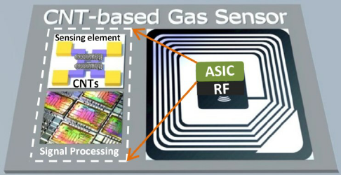
Fig (1). CNT based gas sensor.
CNT based sensors are mostly ubiquitous because of their huge potential for cost saving in fabrication in local synthesis. This paper demonstrates on fabrication method, electrical properties and sensor experimentation for CNT based gas sensors. The tests are performed on two gas compounds air/CO2 and Argon/CO2. The selection of the sensor with CO2 and inert gases is suitable in our study because inert gases are often used for modified atmospheric packaging (MAP) of food products. Freshness of the food can be determined by detecting the amount of CO2 released as a process of degradation of food inside the packages with inert gases. Argon can be used for the test since it is used as a MAP gas for keeping food fresh for longer time.
II. Theory
Though there are many kinds of graphene, due to their distinctive properties single walled nano tubes have tremendous denotation. The designing of carbon nano tubes is made by rolling graphene of single atom thickness considering length to diameter ratio ranging from as high as 1,000,000. Since the finding of nano tubes scientists have discovered enormous applications of them. Compared to other uses, single wall carbon tubes as gas sensors is considered as efficient.
CNTs are carbon allotropes with physical and optical properties. Peculiar properties, like the larger surface area to volume ratio, makes its surface sensitive in various kinds of sensing applications.
A. Structure of CNTs
The quantum chemistry applied to the nature of the bond of the nanotube is specifically delineated by orbital hybridization. The chemical bond of the nanotubes is mainly Sp2 bonds like that of graphite. This bonding structure is stronger than the Sp bond found in the diamond, providing the molecules a distinctive force. Nanotubes naturally align through Van der Waals force as rope like structure. These tubes are often considered as rolling graphene sheets with completely unique built. There are two primary structures namely arm chair and zigzag having more coherence which infer the design of the hexagons over the perimeter. The third kind is Chiral with mirror type bonds. The same is considered in this study.
B. Optical Properties of CNTs
As we know that CNTs are categorized into multi wall and single wall nano tubes. Single wall nano tubes(SWNTs) grab more attention with their optical properties. These are structured by bending a 2D graphene honey comb sheet of 1nm diameter and length of 1 µm. The structure of SWNT is set by a single parameter inferred as chirality. The electrical properties of SWNT are differentiated into metallic or semi conductive based on chirality. Energy band gaps which are controlled by tube diameter(1.2 nm) containing photons corresponding to the wavelength(1550 nm) are being absorbed in a semi conductive SWNT is saturable and recovery time is less than 1ps.
These are manufactured through different processes although after the purification process, high purity SWNTs are dissolved in ethanol and then spread on the surface of quartz’s outer layer.
C. Electronic Properties of CNTs
Carbon is the basis of all organic chemistry, attributable to the flexibleness of its bonding. Carbon-based systems show many alternative structures that are almost like different types of physical properties. These properties are substantial, the results of their size structures. Carbons 3D allotrope plays a vital role in the understanding of electronic characteristics in alternative forms. A honey comb structured engineered from a graphene polygon shape is created from carbon atoms which will have benzene wings off from H atoms that are spherically found. Carbon nano tubes are often obtained by reuniting carbon bonds by rolling graphene in 1D. Therefore, carbon nano tubes solely contains hexagons and are tough of as 1D objects. 3D allocation of carbon is created from C and graphene layers that are bonded by Van der Waals forces.
The structure of graphene reflects its flexibility of electronic properties sp2 hybrids between one S orbital and 2 P orbitals can cause a triangular plane bond between the carbon atoms by 1.42 Armstrong. The σ band is liable for the strengthening of all the lattice structures in allotropes. Hence Pauli.’s formula, these bands exist a filled shell and therefore a broader valency band is created. The potential p orbital that is perpendicular to the structure of the planner bind with neighboring carbon atoms, resulting in the formation of π band. As a result of every p orbital band contains one additional electron, the π is half full.
The exciting feature of Paul Adrien Maurice Dirac fermions is their insensitiveness to external electrostatic potentials attributable to the alleged Klein contradiction, That is the very fact that Dirac fermions may be transmitted with probability one thought he classically prohibited region. In fact , Paul Adrien Maurice Dirac fermions behave unusually within the presence of confining potentials, resulting in the development of Zitter-bewegung, or nervy motion of the wave function. In graphene, these electric potentials may be generated merely by disorder. The sources of disorder in graphene are several and might vary from common effects usually found in semiconductors, like ionized impurities with in the Si substrate, to adatoms and various molecules absorbable within in graphene surface, to more off defects like ripples related to the soft structures of graphene. Due to its eccentric design and electronic convenience, graphene is chemically and productively tailored to numerous methods, like the employment of nitrogen and boron structure in different nano tubes and also the use of various materials that modified the electronic structure. Control of graphene features will be enlarged in new ways that permit graphene- based systems to be developed, that are distinctive to their 2 D properties with magnetic and super conducting properties. Although the graphene field remains inert, the scientific and technical prospects of this new material appears to be enormous. The perception and management of the properties of this material will open doors for a new born ray in electronics.
D. Carbon nano tubes as gas sensors
CNT has been known to be used as adsorbents for heavy metals which is possible due to the high boding of carbon atoms to gas molecules. But the primary concern of them is toxicity which can affect human heath and environment. Nanotube-based sensors possess high sensitivity at low temperature mainly due to its cylindrical shape and high aspect ratio. Hydrogen, ammonia, nitrogen dioxide and carbon dioxide finds its applications. Another limitation to be considered is low reactivity of CNT which can be enhanced by applying PolyAniline[PANI]. [PANI]/SWNT can sense sub parts per million of ammonium, nitrogen dioxide, carbon dioxide, Benzene at room temperature. In general [PANI]/SWNT can be fabricated by using photolithography techniques. Gas sensors suspended in nitrogen dioxide can be removed by heating few minutes, via self-heating and they are decidedly less sensitive to humidity at room temperature. Using distinguished 2 D structure, large surface and chemical stability are reasons for it.
III. DESIGN AND ANALYSIS
The methodology of this paper depends on the principle of creating locally high temperature (up to 900 ° C) using a micro heater on the chip. Fabrication of microheaters in PolyMUMPs commercial process given by MEMSCAP is discussed here. Fig. 2 depicts the orientation of micro heaters containing silicon bridges. Two silicon bridges are separated by distance up to 10µm. The iron films of thickness 3nm and 5 nm which acts as a catalyst are implanted though thermal evaporation. The quartz crystal-based thickness monitor controls the deposition thickness. Prior to the growth of CNTs local thermal annealing has been carried out in order to transform iron films into nano particles maintaining the temperature of about 700° C under atmospheric pressure in inert atmosphere. During the growth of carbon nano tubes the iron nano particles are the catalytic sites. Followed by local synthesis of carbon nanotubes at 900° C at 0.4 bar (C2H4 + Argon environment). The resistance of the silicon bridge determines the temperature of the micro heater that are to be monitored. The arrangement of silicon bridges are in a way that they are perpendicular to precursor flow direction as shown in Fig 4.
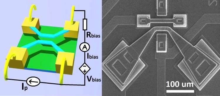
Fig. 2 PolyMUMPS microheaters designed to reach maximum temperature at specific locations where the growth of CNTs will occur.
The main criterion of utilizing external electric field is to arrange the CNT’s growth direction. The electric current which is passing through silicon bridges (Ibias) is being monitored to ensure the connections made by the CNTs. The current passing is limited through bias resistor (Rbias) in CNTs. The carbon nano tubes being the sensing elements forms Si-CNTs-Si structure which is tested as CNTs based gas sensor. The free standing CNTs which are supported by silicon bridges are inter connected to gold pads. The characterizations of CNT based sensors to Argon (Ar) Carbon Dioxide(CO2) and air (78% N2 and 21% O2) are made based on sensitivity and selectivity.
Fig. 3 shows the schematic diagram of sensor test experiments. The changes in I-V characteristics of carbon nano tubes using Wheatstone bridge configurations are noted for denoting CNT based gas sensors when being exhibited to various gas compositions(air/CO2 and Argon/CO2).
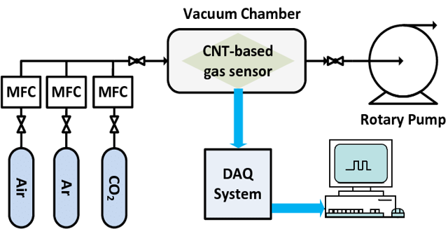
Fig. 3 Schematic diagram of gas detection setup.
IV. RESULTS
Micro heaters are used for notable establishment of Carbon Nanotubes as shown in Fig 4. The surface and side walls of the heating bridge are integrated along with CNT’s. The contact between suspended silicon structures is constituted by nano tubes. This contact is ingrained after ~10 seconds with the speed of about 1µm/s.
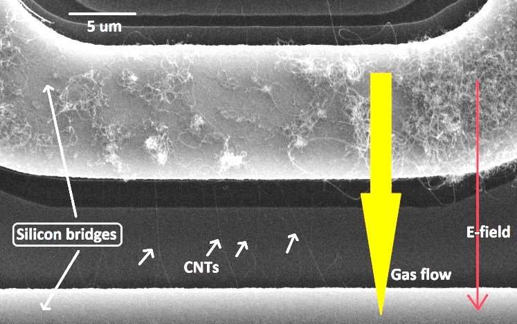
Fig 4. Naotubes connecting the two suspended microstructures to form the chemiresistive gas sensor.
The connections between grown CNTs and silicon bridges are assumed to be resistors and diodes in parallel connection as a result of I V characteristics. The breakdown voltage is ~ 2.3V based on the behavior of Si-CNTs-Si structure. From Fig. 5 Even though reverse bias voltage is given as an input to Si-CNTs-Si structure there is no evidence of reverse conducting current provided reverse bias voltage is less than 10 V.
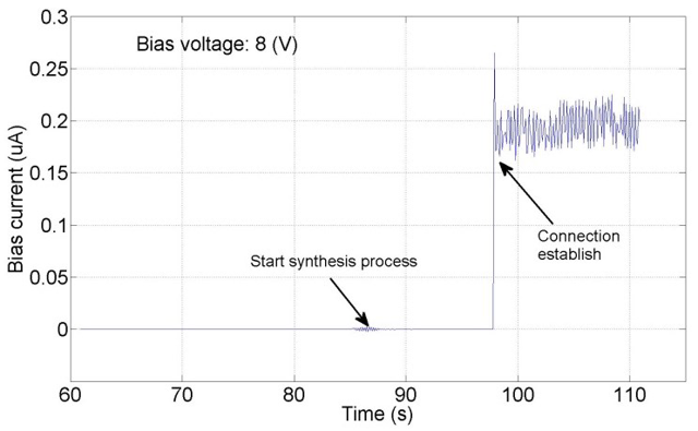
Fig 5. Current bias (Ibias) jump when the connections between Si- bridges are established by CNTs. (Rbias = 40MΩ, Vbias = 8V).
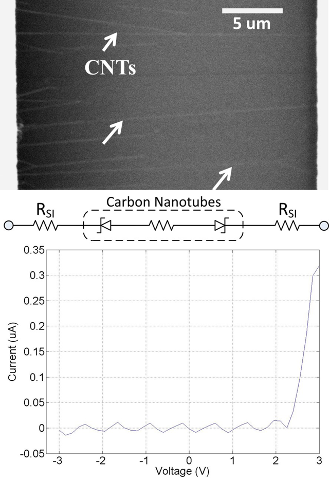
Fig 6. Behavior of I V curve of Si – CNTs – Si structure and equivalent electrical circuit.
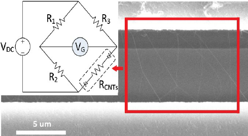
Fig 7. Circuit and graph of CNTs to form chemiresistive gas sensor.
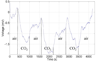
Fig 8. Results from combination of CO2 and air-based CNT gas sensor.
Behavior of Wheatstone bridge voltage Vg when CNTs are continuously exposed to CO2/air and CO2/Argon are shown in Fig 8 and Fig. 9 respectively. For CO2/air combination, Before air being replaced with CO2 at pressure of 1 bar Wheatstone bridge is set to be stable condition (VG = 0). As an effect the I-V graph of carbon nano tubes are altered by CO2 gas.
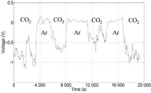
Fig 9. Results from combination of CO2 and Argon based CNT gas sensor.
Unlike CO2/air combination CO2/Argon gives different effect when Argon is replaced with CO2 at pressure of 1 bar. We can observe drop in the voltage of two orders magnitude when compared to CO2/air test.
V. CONCLUSION
A CNT gas sensor prototype constructed by local synthesis is explained. The carbon nano tubes were straight away merged over silicon-based circuits at room temperature. We can infer from the initial test responses of integrated sensors points that carbon nano tubes can also be utilized as sensors tools for carbon dioxide (CO2) more effectively in an Argon atmosphere. However less sensitivity of 0.6 µV/ppm CO2 is observed this methodology can be considered as a favorable application of CNTs into MEMS/CMOS devices to form high sensitive and affordable CO2 sensor for detecting degradation of fresh food.
References
[1] Huy Quoc Nguyen, Bao Quoc Ta, Nils Hoivik, Einar Halvorsen, Knut E. Aasmundtveit. “Carbon nanotube based gas sensor for expiration detection of perishable food” , 2013 13th IEEE International Conference on Nanotechnology (IEEE-NANO 2013), 2013
[2] Spencer, K. C. Humphreys, D. J., “Argon packaging and processing preserves and enhances flavor, fresh-ness, and shelf life of foods,” Cadwallader, K. R. Weenen, H. (Eds.): Freshness and shelf life of foods. ACS Symposium Series (836) 2003: pp. 270–291. J. Clerk Maxwell, A Treatise on Electricity and Magnetism, 3rd ed., vol. 2. Oxford: Clarendon, 1892, pp.68–73.
[3] A. Durairajan, S. Ananthakumar and M. Mohamed Yusuf, Reducing
the emissions from the automobiles by using carbon nano tubes (Nano
Technology), Department of Mechanical Engineering, K.S.R College of
Engineering, Tiruchengode, India,March 2012.K. Elissa, “Title of paper if known,” unpublished.
[4] Michele Magno,Vana Jelicic,Kiran Chikkadi,Cosmin Roman,Christofer
Hierold,Vedran Bilas and Luca Benini, Low-Power Gas Sensing Using
Single Walled Carbon Nano Tubes in Wearable Devices, ETH Zrich,
Zrich, Switzerland,September 2016.Y. Yorozu, M. Hirano, K. Oka, and Y. Tagawa, “Electron spectroscopy studies on magneto-optical media and plastic substrate interface,” IEEE Transl. J. Magn. Japan, vol. 2, pp. 740–741, August 1987 [Digests 9th Annual Conf. Magnetics Japan, p. 301, 1982].
[5] L. Starman and R. Coutu Jr., “Stress Monitoring of Postprocessed MEMS Silicon Microbridge Structures Using Raman Spectroscopy,” Experimental Mechanics (2012): p. 9586-9595.
[6] Bao Quoc Ta, Hoivik, N.; Halvorsen, E.; Aasmundtveit, K.E., “Electrical control of synthesis conditions for locally growth CNTs on polysilicon microstructure,” IEEE-Nano 2011: p. 374377.
[7] Zeila Zanolli and J.-C. Charlier, “Defective carbon nanotubes for single-molecule sensing,” Physical Review B 80 (2009): p. 155447-155453.
[8] Hoefer U., et al, “CO and CO2 thin-film SnO2 gas sensors on Si substrates,” Sens. Actuat. B-Chem. 1994, 22: p. 115–119
Cite This Work
To export a reference to this article please select a referencing stye below:
Related Services
View all


DMCA / Removal Request
If you are the original writer of this essay and no longer wish to have your work published on UKEssays.com then please click the following link to email our support team:
Request essay removal