Uninterruptible Power Supply
| ✅ Paper Type: Free Essay | ✅ Subject: Engineering |
| ✅ Wordcount: 3003 words | ✅ Published: 30 Aug 2017 |

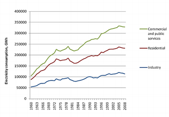 In the United Kingdom over the past half century, the use of electricity has been increasing year on year (Figure 1).
This increase in demand means that the supply of electricity is becoming more critical to the consumer and how much everyday life requires the use of electricity.
Disruption to the supply can cause major issues and potential financial difficulty to many consumers who require a constant supply. Electricity disturbances can come in many different arrangements which affect the AC waveform and influence electrical loads in different ways.

 Common disturbances are shown in Figure 2
Depending on the criticality of the load devices can be placed between the supply and the load to eliminate these issues.
Common devices used to eliminate disturbances are
- Uninterruptible power supplies
- Power Filters/Conditioners
Different UPS systems can be used to eliminate disturbances through different configurations and setups.
Power conditioners operate to illuminate certain aspects of the disturbances but won’t eliminate disturbances like interruptions
UPS systems can incorporate power conditioners to eliminate all these common disturbances to help give a constant supply for consumers.
1.1 Aims
The principle aim of this final year individual project is to design and build an Uninterruptible Power Supply to eliminate interruptions up to 5 minutes. On failure of the supply, the system will pick up the load and continue to provide power until the main supply has returned after 5 minutes
1.2 Objectives
- Research and develop an understand of existing UPS configurations
- Design and build a standby UPS system including
- An AC to DC rectifier to supply an input to a DC Buck Charger
- A DC to DC converter to reduce input voltage to charge retrospective batteries
- A DC to AC inverter to make an AC voltage of 24V RMS
- An AC to AC converter to transfer between the duty and standby supply
- Develop an Arduino interface to control and display UPS parameters including
- Control of the switching of the DC to AC inverter
- Control of the AC to AC transfer switch
- Manual Control of UPS
- Display of UPS circuit position
- Voltage parameter readings for AC and DC
- AC load current and voltage readings
- Battery Temperature readings
- Evaluate UPS and discuss further work
1.3 Motivation
The motivation for this final year project has come from time spent on placement at Phillip66 Humber Refinery working on the maintenance of primarily double conversion and rotary UPS systems. Through this experience, it has given an understanding of the systems and an interest to design and build a UPS.
2.1 UPS Configurations
An uninterruptible Power supply is a system designed to maintain power or provide power when the input power fails or is disrupted. A UPS can be designed as a DC or AC back up, but most common UPS systems in the UK are designed to give AC because this is how electricity is supplied through the grid. [3]
An AC UPS output can be produced using either a rotating machine (Rotary UPS) or a semiconductor based inverter (Static UPS). Batteries are the main energy source for both systems but for rotary systems, other rotating energy sources can be used.

 The UPS configurations as shown in Table 1 shows the different arrangements of a UPS
2.2 UPS Operation
2.2.1 
 Rotary UPS
The rotary UPS generally consists of a motor and generator set but how these are configured depends on of the type of rotary UPS.
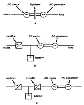
Fixed Flywheel UPS (Figure 3a) [3] [4]
Mains electricity operates an AC motor that is connected through a specially designed flywheel to an AC generator to produce an AC output. While the motor is driving the generator the flywheel rotates which stores kinetic energy. When the main supply fails the kinetic energy in the flywheel continues to turn the generator for a short duration until another supply is provided by a backup generator.
Battery backed (Figure 3B & C)
Mains electricity is converted to DC to charge a battery bank this DC is then used to operate a DC motor directly or through an inverter to an AC motor depending on the configuration. The motor is then directly coupled to a generator to supply the load.
Diesel Backed (Figure 4)

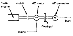 This UPS operates similarly to a flywheel UPS in normal operation an AC motor rotates a flywheel to store energy while a generator is producing power to the output. Instead of an external diesel generator set being used a diesel engine is coupled directly to the AC generator to produce power when the main supply fails.
2.2.2 Static UPS
A static UPS generally comprises of a rectifier, inverter and a battery bank, how these are configured depends on the type of static UPS.

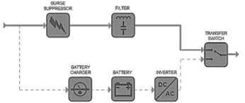 Standby (Figure 5) [5] [6]
In normal operation, a rectifier charges a set of batteries and the input is fed to the output through a transfer switch when the mains fails the transfer switch changes to take the supply from the batteries through an inverter.
Standby-Ferro (Figure 6) [5] [6]

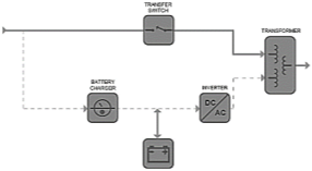 This configuration is very similar to the standby UPS but has a ferroresonant transformer to reduce the time loss of power on a changeover from main to inverter supply, this transformer stores energy in a resonant circuit which supplies up to a half cycle of power to allow time for the inverter to start up and provide power.
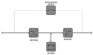 Double Conversion (Figure 7) [5] [6]
 In normal operation, mains electricity is converted to DC to charge the batteries which is then inverted back to AC filtered and supplied to the load. When power is lost the batteries supply the AC through the inverter. The static switch is used in the event that if the rectifier or inverter fails the load can be supplied directly from the load.
Delta Conversion (Figure 8) [5] [6]

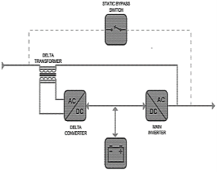 In normal operation two converters are used to regulate current and voltage, the series converter is used to control current and a parallel converter to control the voltage. The converter operates to maintain a constant voltage and current output. When the supply is less than the load requires the batteries are used make up the difference. When too much power is provided the extra is used to charge the batteries through the bi-directional inverter.

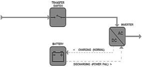 Line Interactive (Figure 9)[5] [6]
In normal operation, the mains is supplied to the output while the bi-directional inverter is charging the batteries. When the main supply fails the inverter changed direction and supplies the load from the batteries.
2.3 UPS Comparisons
To gain a better understanding of the UPS configurations and their capabilities a compassion was conducted as illustrated below (Table 2).
|
UPS Configuration |
Power Rating Range (kVA) |
Cost per VA |
Efficiency |
Application |
|
Standby |
0 – 0.5 |
Low |
Very High |
Interruptions |
|
Standby-Ferro |
3- 15 |
High |
Low-Medium |
Interruptions |
|
Double Conversion |
5-5000 |
Medium |
Low-Medium |
Transient, Interruptions, Sag/Swell, Distortion |
|
Delta Conversion |
5-5000 |
Medium |
High |
Transient, Interruptions, Sag/Swell, distortion |
|
Line Interactive |
0.5-5 |
Medium |
Very High |
Interruptions |
|
Flywheel Rotary |
25-2500 |
Medium |
Medium to High |
Transient, Interruptions, Sag/Swell, Distortion |
|
Battery Backed Rotary |
Medium |
Medium to High |
Transient, Interruptions, Sag/Swell, Distortion |
Table 2: UPS Configuration Comparison [5]
2.4 Project Reasoning
A standby UPS system was chosen due to its low cost, its simplicity and because it covers a single disruption. This type of UPS is basic to remove loss of power and to bridge the gap between power loss and back up operation starting
3.1 Work Breakdown Structure and Network Diagram
A WBS is a key project deliverable that organises work into manageable sections and is the foundation of any project plan. All the project deliverables are selected and organised into key areas of activity. [7]
A network diagram shows the sequence of activities which are in the WBS in order of time, these are then used to develop a Gantt chart.
The WBS (Appendix 9.2.1: WBS) separated the project into 5 main sections which were then subdivided to develop a network diagram (Appendix 9.2.2: Network Diagram)
- Research
- Design
- Programming
- Build testing
- Report/ Presentation
3.2 Project Plan
A project plan was developed as a Gantt chart from the network diagram, the time scale for the project was set to begin in September and complete the development of the UPS by December. This giving two months before the deadline to complete final checks and adjustments.
The project plan was reviewed weekly and updated as the progress of the project developed.
3.3 Monthly Reports
A monthly report was conducted to record and document my project progress on a regular basis, each monthly report is attached in Appendix 2 – Project Planning. This report involved a document of the work I had conducted the month before and also a plan of what I would be doing for the next month including a number of hours that would be spent.
3.4 Project Progress Review
A PPR was conducted on Friday 2nd December by Dr Joe Cole this was designed as
For the design and building of this standby UPS, it has been split into individual circuits to ease the understanding and to show the importance of each aspect of the UPS. The UPS has been divided as follows
- AC Rectification
- DC Inverter
- Battery Charging
- Transfer Switch
- Control of the UPS
4.1 Bridge Rectifier (AC >> DC)

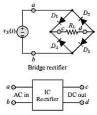
4.1.1 Calculation & Theory
An AC to DC converter is required to utilise the mains AC voltage to charge a set of batteries for use when the AC signal is lost.
A rectifier circuit can be designed to utilise either full or half of the AC waveform, this can be achieved through the use of diodes or thyristors.
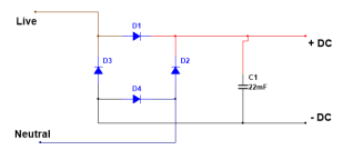
Figure 10 shows the circuit configuration of a bridge rectifier which can use either component.
The difference between using diodes and thyristors is the control over the voltage on the output, diodes give an output equal to the peak voltage of the AC waveform and thyristors voltage depends on the firing angle used to turn the thyristors on.

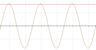 To achieve a pure DC voltage filtering is required to remove the ripple of the sinusoidal waveform. Figure 11 shows how the DC can be filtered to give a pure DC voltage through the use of a capacitor.
For this project, a constant DC voltage equivalent to the peak AC waveform can be used to supply the Buck Battery Charger because this will reduce the DC voltage to the required voltage to charge the retrospective batteries.
For the purpose of this project, a diode full wave bridge rectifier can be used to supply 34V to the buck battery charger.
4.1.2 Simulation
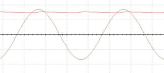
The circuit in figure 4.1.1 was modified to add a smoothing capacitor then it was built in Multisim as shown in Figure 9which gives the output as shown in Figure 13.


4.1.3 Building and Testing

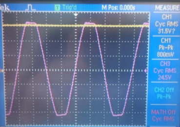 After simulation was complete the circuit was built on a breadboard so that its operation could be tested in practice before a PCB was designed. The practical testing is shown in Figure 14.
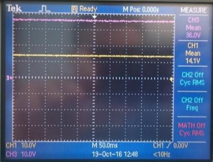
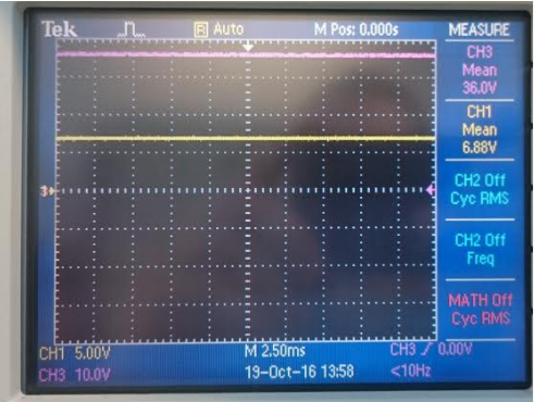
It can be seen that the incoming 24V AC supply is changed to DC through the bridge rectifier which is shown as the peak voltage on channel 1 as 31.5 V DC

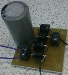
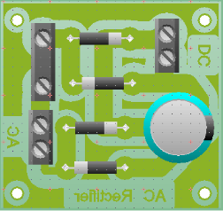 Once the circuit was tested on a breadboard it was then produced on a PCB, this was soldered using the same components and tested to give the same results as in Figure 14. The PCB design and finished PCB can be observed below (Figure 15/16)

4.2 Inverter (DC >> AC)

4.2.1 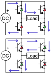 Calculation & Theory
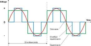
To convert the DC voltage stored in the batteries to make AC voltage a DC to AC inverter is required. There are three main types of DC to AC inverter which depend on the AC output waveform, these are square, modified sine and pure sine wave.
The difference between the modified sine and the pure sine wave is that the modified sine rests on the 0 line for a small amount of time then either rises or falls whereas the sine wave goes straight through the 0 line. (Figure 17)
For this application, a sine wave as close to the mains is required so a modified sine wave will be produced which will be filtered to make a sine wave.

 To change DC to AC an H bridge is required similar to that of an AC to DC converter. As can be seen in Figure 19 the switching of the H Bridge changes the current flow through the load and so creates AC.

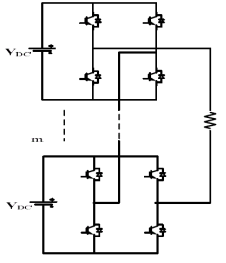
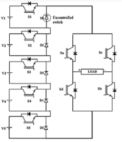
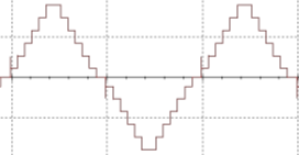
 The issue with this circuit is that it will give an AC square wave, to adapt this to make a modified sine another bridge is required Figure 18to introduce a voltage step and make a multilevel inverter. Each bridge is use to add a square wave on top of each other so that an output Figure 20
 can be produced. With an increase in H-bridges, this means an increase of switches and DC sources.
The DC sources are required to make an AC RMS voltage equivalent to that of the mains input (24V RMS). The peak voltage of the AC waveform has to be matched by the total voltage of the DC, this means that a total DC voltage can be calculated by equation 1 which gives a value of 33.94 V.
 To achieve this voltage exactly through the use of DC sources would be hard so a voltage higher would be best through the use of four 9V or six 6V batteries used to get 36V, this would mean that by using six 6V batteries smaller steps are achieved but more bridges are required which would be more accurate than using 9V steps and having fewer bridges.
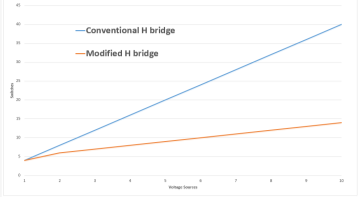
 To eliminate the repeated use of bridges a modified multilevel inverter circuit (Figure 21) can be developed to use 1 bridge and switch on each source as required so that switch numbers can be reduced from 24 switches to 10 switches.
 The reduction of switches can be observed through a comparison of the conventional and modified H-bridge. (Figure 21).
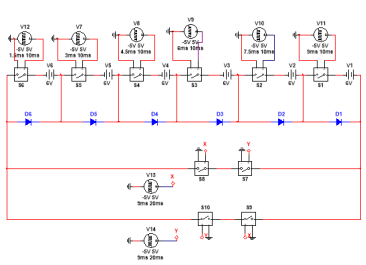
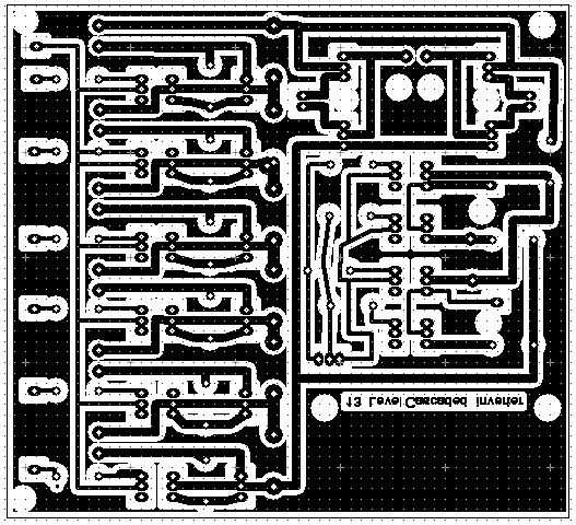
For this inverter, it will be designed as a 13 level modified multilevel inverter which requires 8 control signals to switch on each 6V source and also to change the polarity across the load.
4.2.2 Simulation
A 13 level modified cascaded inverter was built in Multisim using 8 pulsed signals that represent the signals obtainable from the microcontroller. This gives a modified sine wave output that is operating at 50Hz with a peak to peak of 72 V.

4.2.3 Testing
4.3 Battery Charger (DC >> DC)
4.3.1 Calculation & Theory
To charge the six 6 V batteries for the inverter and single 12-volt battery to supply the Arduino it is required to reduce the 34V produced from the AC rectifier to a suitable level for the retrospective batteries to charge. This is normally 1.15 times the voltage of the rated battery voltage which gives 6.9 volts and 13.8 volts which are confirmed in the datasheet for each battery.
To reduce the DC voltage a chopper circuit is required, these can be categorised as either switched or linear, and to understand the characteristic a comparison of both is shown below [8] (Table 3).
|
Linear |
Switched |
|
|
Function |
Can only reduce voltage |
Can increase or decrease voltage depending on design |
|
Efficiency |
As difference in voltage increases efficiency decreases |
High efficiency |
|
Complexity |
Low usually only requiring a regulator and capacitors |
Medium to high due to inductor, capacitor calculations |
|
Cost |
Low |
Medium to high depending on design |
|
Output Ripple |
Low |
Medium to high due to switching rate |
Table 3: Chopper Comparison [8]
For best efficiency a switched inverter will be used, this is required to give each battery half an amp of current at 6.9 Volt and 13.8 volts.
4.3.2 Simulation
4.3.3 Testing
4.4 Transfer Switch (AC >> AC)
4.4.1 Calculation & Theory

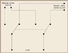 An AC to AC converter is required to change the supply to the output between mains voltage and back up supply from the DC – AC inverter.
This type of AC converter works as a switch to turn either AC source on respectively when it is required (Figure 23), other types of AC to AC converter can be used to change aspects of the AC waveform but this is not required in this application.
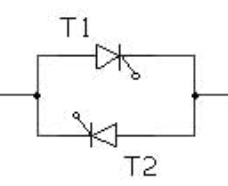 A contactor or a semiconductor device circuit can be designed to make this transfer switch, each of which has its advantages but for this project, a semiconductor device was used, the common devices use to make an AC – AC converter are SCR’s or thyristors.
 To utilise either device a double circuit of back to back devices is used so that each half of the cycle is seen at the output. (Figure 24).
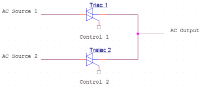
 To prevent using 2 SCR’s or thyristors back to back, a triac can be used to do this job instead. This means that the use of two triacs with a common output and separate inputs can be used as a transfer switch. (Figure 25)
4.4.2 Simulation
To show the operat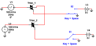 ion of the transfer switch 2 different AC signals of different frequencies are used to show the transfer. (Figure 26).


 When the control signal is supplied to Triac 1 the output waveform is shown as 25Hz but when the control signal is changed to Triac 2 the output changes to 50Hz. (Figure 27)
To isolate the Triac from the microcontroller an optocoupler will be used so that in the event of a fault the microcontroller doesn’t come in contact with the AC voltage
4.4.3 Testing
The transfer switch was built on a prototyping board using two TIC246M Triacs which are then operated through two MOC3021 triac optocouplers, these use the AC signal to turn on each triac.
To test the transfer switch a method similar to that of the simulation was adopted, but instead of using 2 different frequencies, 2 different phases where used then the output was compared to each to show that the transfer switch is operational.

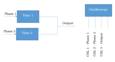 Due to the risk of shorting two phases if an issue occurred each side of the transfer switch was tested for operation individually. Once this was tested and operational the input signal for each phase was placed on channel 1 and 2 of the oscilloscope and the output positioned on channel 3. (Figure 28). This meant that as each triac was turned on it could be compared with the corresponding input to ensure the triac was operating as required. As we see below figure 4.4.3.2 shows the output when triac 1 is operating and figure 4.4.3.3 shows when the second is operational.
When the transfer switch was tested and operational a PCB design was developed on circuit wizard, this also incorporated a CT to measure the output current and a bridge rectifier chip to take a reading of the output voltage peak voltage. These would be sent to the microcontroller to display.
Cite This Work
To export a reference to this article please select a referencing stye below:
Related Services
View allDMCA / Removal Request
If you are the original writer of this essay and no longer wish to have your work published on UKEssays.com then please click the following link to email our support team:
Request essay removal