Methodologies of Microwave Amplifier Design
| ✅ Paper Type: Free Essay | ✅ Subject: Engineering |
| ✅ Wordcount: 922 words | ✅ Published: 30 Aug 2017 |
2.1 ACTIVE DEVICE SELECTION
This chapter discusses various methodologies used in the design of single stage microwave amplifiers. Reaching the desired goals of gain, power loss and noise performance requires first selecting a suitable active device (transistor) that meets these goals. The rapid advances in transistor fabrication have permitted the traditional Si transistors to operate in the GHz re- gion. the increase for higher frequency operation drove the innovation of new novel devices with new materials, architectures and geometries Possibly the most significant difference be- tween microwave transistors and the lower frequency ones is in the area of materials. Although low-frequency transistors are fabricated mostly from silicon, the use more costly compound semiconductors like gallium arsenide (GaAs) and indium phosphide (InP) proves to be more economical at microwave frequencies because of their performance advantages over silicon. The demand for higher frequencies also produced sophisticated material configurations like the heterojunction transistors which have no low-frequency counterparts.
At low frequencies, microwave transistors can be broadly categorized into: the bipolar junc- tion transistors (BJTs) and the field-effect transistors (FETs). At lower frequencies, FETs con- tains the junction FET (JFET) and the metal oxide FET (MOSFET), structural characteristics limits their high frequency operation. GaAs metal semiconductor FET pushed the frequency of operation well into the GHz region. However, in the intervening decades, bipolar device caught up and now it is common to find BJT’s operating at the GHz region.
The selection of a suitable transistor for the required application is based on the targeted goals of gain, noise and power loss performance. In the following sections, the GaAs HJ-FET transistor NE3210S01 from Renessa Electronics will be used to illustrate the various meth- ods for selecting the appropriate terminations used in constructing matching networks for both narrowband and wideband operation.
2.2 MATCHING NETWORKS TOPOLOGIES
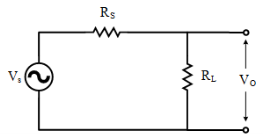
Impedance matching involves transforming one impedance to the other. This process is useful in circuits where the mismatch between the source (ZS) and load (ZL) prevents maximum power transfer. Theorem states that for a maximum transfer of power from source to load. Load impedance (ZL) must be equal to the complex conjugate of the source impedance. Complex conjugate is complex impedance having the same real part with an opposite imaginary one. For example, if the source impedance is ZS =R+jX, then its complex conjugate must be ZL =R-jX. For a pure resistive load, equations (2.1) and (2.2) aided with Fig.2.1 shows that a maximum
4
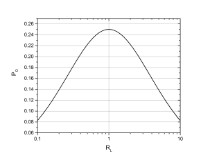
power transfer occurs when RL=RS.
 VO= VS
L
RL
 + RS
+ RS
RL
(2.1)
PO= V2
S(RL+ RS)2
(2.2)
 (a)
(a)
(b)
Figure 2.1: (a) Pure resistive circuit with VS=1V and RS=1Ω, (b) Maxim power is delivered to the load when RL=RS
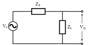
 The same concept can be applied to AC circuits with complex load and source. Equation.2.3 aided with figure Fig.2.2 shows that a maximum power transfer to the load occurs when XL= XS. The value of the power delivered to the load is given by:
1|VS|2 –RL

 PO= 2 (R
+ RL
)2 + (XS
+ XL
(2.3)
)2
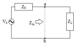
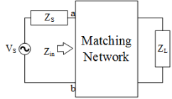
 Where the resistance RS and RL and the reactants XS, XL are the real and imaginary parts of ZS and ZL. The target in applying impedance matching to make the load impedance look like the complex conjugate of the source impedance to attain maximum power transfer to the load. This is shown in Fig. where a matching circuit is placed between points a,b shown in Fig to transfer the load impedance to the complex conjugate value of the source impedance. Since we are dealing with reactances, which are frequency dependent, the matching can occur only at single frequency. That is the frequency at whichXL= X–and, thus, cancellation or resonance occurs. At the surrounding frequencies, the matching becomes worse. This is the main problem in broadband matching where perfect or near perfect matching along the required bandwidth is required. The methods for narraowband and wideband matching is presented later in this chapter.
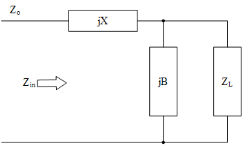
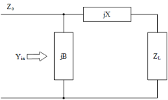
In Fig.2.3b, numerous topologies can be used as a matching network. The shape of the topology can vary from a simple L, πor T networks to a complex ladder circuit or filter design. The concept of matching network can be explained using the two simple L-Matching topologies shown in Fig.2.4a,2.4b. Both B and X values in Fig.2.4 must be chosen to satisfy the condition ZL=ZS*. To achieve this condition, both analytical methods, mostly with the aid of a computer, and graphical procedures, using the Smithchart, can be used.
(a)
(b)(c)
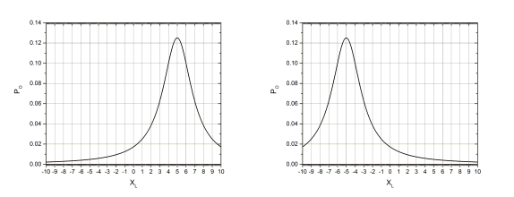
Figure 2.2: (a) AC circuit with complex ZS and ZS, (b) For XS=j5, Maxim power is delivered to the load when XL=-j5 (c) For XS=-j5, Maxim power is delivered to the load when XL=j5
For the case of RL ¿ Ro, the topology of Fig.2.4a is preferred, where B and X are given by:

 RL 22
RL 22
XL±
 B=
B=
ZoRL+ XL−ZoRL
(2.4)
R22
L+ XL
X= BZoRL−XL
1 − BXL
(2.5)
For the condition of RL¡Ro the topology of Fig.2.4b is used with B and X given by:
 1 Zo−RL

 B= ±
B= ±
oL
(2.6)
 X= ± RL(Zo−RL) −XL(2.7)
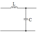
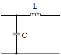
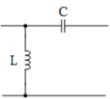
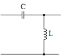
In both topologies of Fig.2.4, B and X represent either an inductor (L) or capacitor (C). The result is four simple L-matching networks as shown in Fig.2.5.
 (b)
(b)
Figure 2.3: (a)Circuit before the matching network(b) Circit after adding the matching network.
 (a)(b)
Figure 2.4: L-Matching topologies, a) used when RL ¿ Ro, b) used when RL ¡ Ro
2.3 NARROWBAND DESIGN METHODOLOGIES
- Analytical Solution
- Graphical Solution
- CAD Solution
- WIDEBAND DESIGN METHODOLOGIES
- Analytical Solution
- Graphical Solution
- CAD Solution
 (b)
(b)
(c)(d)
Figure 2.5: Four basic L-matching Networks
Cite This Work
To export a reference to this article please select a referencing stye below:
Related Services
View all


DMCA / Removal Request
If you are the original writer of this essay and no longer wish to have your work published on UKEssays.com then please click the following link to email our support team:
Request essay removal