Interlayer Effect: Si-based Double Junction Tandem Solar
| ✅ Paper Type: Free Essay | ✅ Subject: Engineering |
| ✅ Wordcount: 824 words | ✅ Published: 31 Aug 2017 |
Investigation of Interlayer Effect on Si-based Double Junction Tandem Solar Cell
Abstract: – Silicon-based double junction tandem solar cell was fabricated and simulated using wxAMPS software. Nano structure of SiO2/ Si3N4 interlayer was inserted between the silicon and InGaN junction to investigate the effect on the quantum efficiency of the Si-based solar cell. The quantum efficiency characterizations were studied under AM1.5 solar spectrum at 300o K. SiO2 was found to be an excellent interlayer for Si-based double junction tandem solar cell compared to Si3N4 and exhibit better quantum efficiency. The addition of SiO2 and Si3N4 nano structure interlayer between the Si and InGaN improved the Jsc by 5.79% and 2.21% respectively compared to the absence of interlayer.
Key-Words: –Silicon solar cell, interlayer, silicon dioxide, silicon nitride, quantum efficiency, wxAMPS
1 Introduction
Due to its low material cost and ease of manufacturing, silicon-based solar cells are preferred for energy conversion. Advances in the technology have significantly improved the overall performance of silicon solar cells. Besides, Si has better cooling capability compared to sapphire [1]. Si has larger thermal conductivity which promises much faster thermal dissipation [2]. Since solar cells operate under high temperature, this characteristic is strongly desired. Indium gallium nitride (InGaN) is one of the best semiconductor materials for optoelectronics which can operate in high-temperature. In addition, InGaN is a widely used for multi-junction tandem solar cells with high conversion efficiency and shown a better resistance to radiation damage compared to other materials. It provides variety of band gap energies as the band gap changes with the In-Ga ratio. Due to its potential in cost reduction and faster thermal dissipation, researchers are committed to study InGaN-on-Si technologies.
As Si and InGaN is having large relative lattice mismatch, the conversion efficiency of the device is limited. This issue leads to phase separations. Because of that, suitable interlayer or absorber layer is desired to ensure each layer to match. Thermal lattice mismatch was reported by Krost et. al in 2002 stating that cracking of GaN on Si usually occurs due to the large thermal mismatch of GaN. The thermal stress can be reduced significantly by insertion of low-temperature AlN interlayers, introducing multiple AlGaN/GaN interlayers, and growing on prepatterned substrates [3].
The interface traps at the nitride/Si interface exhibit dissimilar properties from those at the SiO2/Si interface in some aspects. Thermally grown SiO2, the currently established gate dielectric for Si-based MOS devices, possesses remarkable electronic properties that are unmatched by other materials. Both SiO2 and Si3N4 are equally transparent even for high energy edge UV band of solar spectrum. SiO2 is highly technically established materials as a passivation layer for Si based MOS technology and it may also be used for integration of PD technology [4]. Si3N4 is also potential coating materials against degradation of detecting device even in high radiation environment and temperature [5].
Implementation of double junction solar cell is one of the alternatives in enhancing the output characteristic of solar cell [6]. Users demand a better efficiency and higher output current of solar cell. Thus, we investigated the structure of InGaN-on-Si solar cell with the presence of different interlayer (SiO2 and Si3N4) which was inserted between Si and InGaN layer to intensify the light conversion in the cell. This structure enables the increase of current of both top and bottom cell by reducing the recombination effects [7]. In this paper, we focused on the quantum efficiency which is one of the criteria that must be considered as we can evaluate the amount of current that the cell will produce when exposed to sunlight.
2 Experimental Procedure
The structure as shown in the Fig. 1 was fabricated using wxAMPS software which was developed by Prof. Rockett and Dr. Yiming Liu of UIUC and Prof. Fonash of PSU. The solar cells were grown on a n-type silicon substrate. Three different experiments have been conducted; without interlayer, with SiO2 interlayer and with Si3N4 interlayer.

Fig. 1- Structure of the solar cell
Composition of In0.4Ga0.6N with Eg=1.99 eVwas used in all three experiments. The output characteristics were studied under AM1.5 solar spectrum at 300oK. InGaN is chemically a n-type semiconductor because of the presence of nitrogen in the composition. Mg is used to dope the InGaN in order to make it p-type [8].
3 Result and Discussion
Fig. 1 presents the internal quantum efficiency of the three conducted experiments.

Fig. 2- Internal Quantum Efficiency
From Fig. 2, insertion of SiO2interlayer shows better IQE compared to Si3N4 and without interlayer. The difference in the IQE can be seen at high energy spectrum. The difference is due to the recombination at the surface of the cells. When carriers are generated near the surface, and since blue light for example is absorbed very close to the surface, quantum efficiency at high energy edge which absorbed very close to the surface will be affected by the front surface recombination. Presence of interlayer leads to a higher generation rate and it is more significant at the wavelength λ<600 nm.The IQE also affected by reflection and diffusion length. When SiO2/ Si3N4is introduced between the Si and InGaN layer, the absorption is further improved and enhances the diffusion length. The highest quantum efficiency is recorded at the wavelength of 650-700 nm. The surface recombination and diffusion length in the bottom cell tends to shift the peak to lower energy edge. The properties of SiO2 and Si3N4 itself differs from each other. SiO2 has a refractive index of 1.57 while Si3N4 with refractive index of 2.05. SiO2 permits selective diffusions into silicon wafer.

Fig. 3- Current density without interlayer
Since the solar cells are made up of p-type and n-type semiconductors, electrons from the n-region near the p–n junctionlikely to diffuse into the p region. As these electrons diffuse, positively charged ions (donors) are left in the n-region. On the other hand, holes from the p-type region near the p–n junction start to diffuse into the n- region. As we analyze the current density behavior based on the structure in Fig. 1, the bottom cell (Si) which is stacked with InGaN layer determines the current density with the presence/absence of interlayer. It can be seen that recombination that occur in the bottom cell affected its total performance. Besides, the in-plane lattice mismatch between Si and InGaN was reported by Henini in his book. Direct growth of InGaN layer on Si (without buffer or interlayer) gives in-plane mismatch from -7.81% to -17%; depending on the content of Indium and Gallium [9]. Direct growth of InGaN on Si makes some part of the InGaN diffused into the Si. Carrier recombinations at localized states arise due to this lattice mismatch which leads to lower Jsc. Besides, cracking of GaN on Si usually occurs due to the large thermal mismatch of GaN. This lattice mismatch effect can be reduced by inserting interlayer which can reduce the thermal stress between the junction of InGaN and Si. GaN-based semiconductor is not well suited for direct growth on Si.

Fig. 4- Current density for Si3N4 interlayer
From Fig. 4, the behavior of the current density with Si3N4 interlayer is almost the same with no interlayer but it gives lower recombination rate hence produces greater current-density compared to the one in Fig. 3. At 0.08 µm-0.1 µm, it can be observed that Jn and Jp stay constant at a deeper position from the bottom cell. The final alignment and function of InGaN cell is strongly dependent on the starting substrate type, orientation, substrate pre-treatment, type of buffer or inter layer and growth conditions. High recombination rate as shown in Fig.3 and Fig. 4 is not desired. Thus, Si3N4 is not so suitable to be used as an interlayer between Si and InGaN.
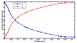
Fig. 5- Current density SiO2 for interlayer
Fig. 5 shows the current density at the bottom cell when SiO2 is used as interlayer. Unlike Si3N4, cells with SiO2 as its interlayer give less recombination rate. The type and magnitude of recombination processes in the cell greatly affected the minority carrier lifetime and the diffusion length. The recombination rate will depend on the number of defects present in the material. Defects here may refer to the doping concentration, dopants or the properties of the material itself. Less interface defects are shown by SiO2 and this is proven by nowadays Si fabrication technology which uses SiO2 as gate interface. Even though both SiO2 and Si3N4 are equally transparent for high energy edge of solar spectrum, but the interface traps at the nitride/Si interface exhibit contradictory properties from those at the SiO2/Si interface in some aspects.
|
No interlayer |
SiO2 interlayer |
Si3N4 interlayer |
|
|
Voc (V) |
1.5886 |
1.6371 |
1.5912 |
|
Jsc (mA/cm2) |
6.4706 |
6.8454 |
6.6136 |
|
FF (%) |
48.439 |
52.2130 |
48.8326 |
|
Efficiency (%) |
4.9791 |
5.8513 |
5.1390 |
Table 1- Output characteristics of the solar cell based on different interlayer
The output characteristics as shown in Table 1 are relatively important in determining the performance of solar cells based on different interlayer. It can be seen that SiO2gives a higher Voc, Jsc, fill factor and efficiency compared to Si3N4. The addition of SiO2/Si3N4 nano structure interlayer between the Si and InGaN improves the Jsc by 5.79% and 2.21% respectively compared to the absence of interlayer.
4 Conclusion
The effect of different interlayer on Si-based solar cell is studied. InGaN is not well suited fordirectgrowthonsiliconsubstrate. SiO2 has shown to be an excellent interlayer between Si and InGaN cell. It appears that suitable choice of interlayer is important to match the top cell and the bottom cell. The interlayer also will give a significant effect on its quantum efficiency and total current density.
5 Acknowledgement
I would like to thank Pusat Penyelidikan dan Inovasi UMS and Kerajaan Malaysia for the funding of this project (Project code: FRG0307-TK-1/2012).
References:
- C.Y.Liuet al.,”Nitride-based concentrator solar cells grown on Si substrates”, Solar Energy Materials & Solar Cells117(2013)54–58
- Miro Zeman & Janez Krc. “Electrical and Optical Modelling of Thin-Film Silicon Solar Cells.”MRS Proceedings. Vol. 989. No. 1. Cambridge University Press, 2007.
- Krost, Alois, and Armin Dadgar. “GaN-based optoelectronics on silicon substrates.”Materials Science and Engineering: B93.1 (2002): 77-84.
- Eujune Lee et, al., IEEE Electron Device Letters, Vol. 30, No. 5, May 2009
- Sinje K-C et. al., 26th EU PVSEC – European Photovoltaic Solar Energy Conference & Exhibition, 05-09 Sept., 2011
- L. A. Vilbois et al., “Simulation of a Solar Cell Based on InGaN”, Energy Procedia 18 ( 2012 ) 795 – 806
- El Gmili, Y., et al. “Multilayered InGaN/GaN structure vs. single InGaN layer for solar cell applications: A comparative study.”ActaMaterialia61.17 (2013): 6587-6596.
- Islam, Rafiqul, et al. “MOVPE Growth of InxGa1-xN(x~0.4) and Fabrication of Homo-junction Solar Cells.”Journal of Materials Science & Technology(2012).
- Henini, Mohamed. “Molecular beam epitaxy from research to mass-production”, Newnes (1996): 33-36.
- Chang, J-Y., et al. “Numerical Investigation of High-Efficiency InGaN-Based Multijunction Solar Cell.” (2013): 1-1.
- Despeisse, M., et al. “Resistive interlayer for improved performance of thin film silicon solar cells on highly textured substrate.”Applied Physics Letters96.7 (2010): 073507-073507.
- Araújo, Andreia, et al. “Role of a disperse carbon interlayer on the performances of tandem a-Si solar cells.”Science and Technology of Advanced Materials14.4 (2013): 045009.
- Liu, Yiming, Yun Sun, and Angus Rockett. “A new simulation software of solar cells—wxAMPS.”Solar Energy Materials and Solar Cells98 (2012): 124-128.
- Liu, Yiming, Yun Sun, and Angus Rockett. “Batch simulation of solar cells by using Matlab and wxAMPS.” InPhotovoltaic Specialists Conference (PVSC), 2012 38th IEEE, pp. 000902-000905. IEEE, 2012.
Cite This Work
To export a reference to this article please select a referencing stye below:
Related Services
View all


DMCA / Removal Request
If you are the original writer of this essay and no longer wish to have your work published on UKEssays.com then please click the following link to email our support team:
Request essay removal