Frequency Swept Source using Xilinx DDS Compiler
| ✅ Paper Type: Free Essay | ✅ Subject: Engineering |
| ✅ Wordcount: 923 words | ✅ Published: 31 Aug 2017 |
Keywords-frequency swept source; chirp signal ; DDS Compiler;
This module was designed as a part of the coursework assignment of ECE 580B4 FPGA Signal Proc/Software Defined Radio. The purpose of this assignment was to design a frequency swept source which will be extensively used in testing the Digital FIR filters that are to be designed and implemented as a part of the future coursework.
A. DDS IP Core Compiler
The Xilinx DDS core compiler implements high performance phase generation and phase to sinusoid circuits with AXI-4 stream compliant features. The core sources sinusoidal waveforms for use in many applications. This module comes with an inbuilt sine and cosine Look up table and a phase generator. For the purposes of this assignment, the DDS compiler was configured to receive a streaming phase input and the phase width resolution is set to 8 bits to make the design more space efficient and to make the simulations run faster.
B. Frequency swept Source Design
The Frequency Swept source is coded as a synthesizable Verilog module. In this Verilog Module, The DDS Compiler was instantiated and appropriate phase data is streamed by feeding the data into the s_axis_phase_tdata. s_axis_phase_tvalid is always set to 1 for the purposes of this assignment.
The frequency swept source is expected to sweep from 1Mhz to 10 Mhz in 10 micro-seconds. This basically translates to an increment of 1Mhz in every microsecond. So, initially the increment has been calculated to generate a 1Mhz signal and then the increment is ramped up linearly to generate the desired chirp signal. The following expression has been used to derive the phase increment value.
Fout = fclk* (dt)/ (2^(B));
Here, fout is the output frequency, fclk is the clock frequency, dt is the phase increment and B refers to the phase width. The above equation, for an 8bit phase width, 100 Mhz source to generate a 1Mhz output signal basically expects a phase increment of 2.56. But in this design this has been rounded off to 3. So, a phase increment of 3 refers to an output of 1Mz signal and a phase increment of 6 refers to an output of 2Mhz signal etc. The value of phase increment should realistically increment upto 25.6, so this number will be rounded off to 25. Now, is basically comes down to generating 22 different values for phase increment in a matter of 10 microseconds. In out design, the timescale has been set to 1ns. Now to figure out the delay to increase the value of phase increment in steps of 1, we need to impart a suitable amount of delay. This delay is calculated as shown below
Delay = [10u/(22)] * 10^3 nano seconds. [Assuming a delay of one unit refers to one nano second].
The value of delay comes out to be 454.54 cycles. So, basically, we increase the value of phase-increment in steps of 1 from a starting value of 3 after every 455 clock cycles. This makes sure we are getting appropriate ramping up of the phase increment value to generate the desired sweep.
module freq_sweep( input clk,
output reg [7:0] sin,
output reg [7:0] cos
);
reg[7:0] phase_data;
wire phase_valid;
wire [15:0] nco_data;
wire nco_valid;
integer i;
assign phase_valid =1;
initial begin
phase_data = 3;
end
dds_compiler_0 DUT( .aclk(clk),
.m_axis_data_tdata(nco_data),
.m_axis_phase_tvalid(nco_valid),
.s_axis_phase_tvalid (phase_valid),
.s_axis_phase_tdata (phase_data)
);
always @(posedge clk) begin
if (phase_valid == 1) begin
sin = nco_data [15:8];
cos = nco_data [7:0];
end
end
always begin
for (i=3; i<=24; i=i+1) begin
#454.545454;
phase_data = i;
end
end
endmodule
module testbench();
reg clk;
wire [7:0] sin;
wire [7:0] cos;
freq_sweep freq1 (.clk(clk),
.sin(sin),
.cos(cos)
);
//100M source
initial clk = 0;
always
#5 clk = ~clk;
endmodule
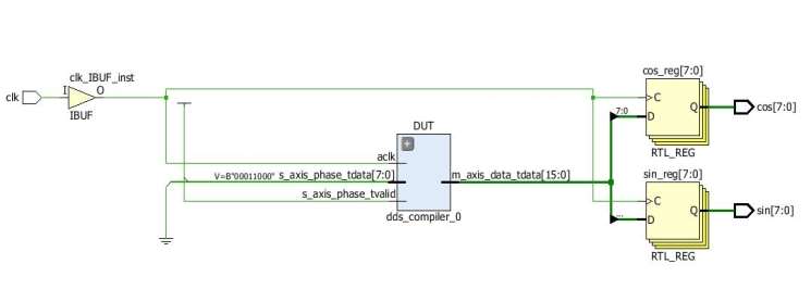
Fig 1.1
The Design was synthesized using the Xilinx Vivado tool. The synthesized schematic (block diagram) is shown in Fig 1.1. The schematic shows two 8 bit output registers which basically generate a sine and a cosine chirp signal. The only input to this module is a clock pulse. It can be seen from the schematic that the phase_valid pin is permanently shorted to Vdd , this has been done just for simplicity and traditionally a more robust logic should be written to determine the validity of the phase. And it can be seen that the phase data has been connected to Vdd and ground through a switch and this switch turns on and off based on the value that is assigned to this 8bit bus.
The generated chirp signal is shown in the below figures.
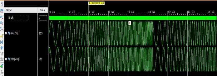
Fig 1.2
Fig 1.2 clearly shows the frequency sweep of 1Mhz to 10 Mhz which takes place in a duration of 10 us.
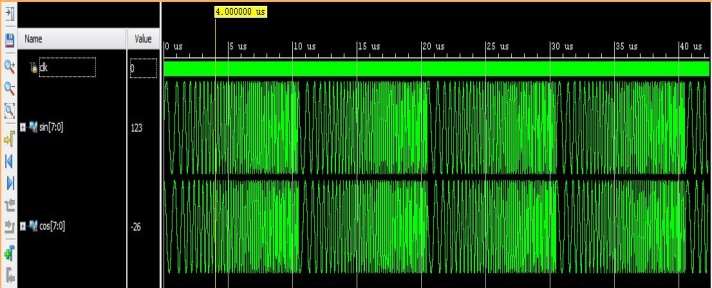
Fig 1.3
Fig 1.3 establishes the fact that the signal is periodic with a period of 10us which is desired as per the specification
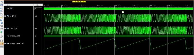
Fig 1.4
Figure 1.4 re-establishes the fact the frequency sweep happens as per designed spec while the phase increment is ramped up linearly through the duration of 10.
The Frequency swept source was designed using the Xilinx DDS IP core. Xilinx vivado tool was used for the purposes of simulation and synthesis. The design has been tested for both behavior and synthesis.
References
 Digital Signal Processing with Field Programmable Gate Arrays, 4th ed. by Uwe Meyer-Baese. Springer, 2014
- Xilinx DDS Comlpiler v6.0 LogiCORE IP Product Guide
Cite This Work
To export a reference to this article please select a referencing stye below:
Related Services
View all


DMCA / Removal Request
If you are the original writer of this essay and no longer wish to have your work published on UKEssays.com then please click the following link to email our support team:
Request essay removal