Design of Manchester Serial Data Communications Channel
| ✅ Paper Type: Free Essay | ✅ Subject: Engineering |
| ✅ Wordcount: 4345 words | ✅ Published: 31 Aug 2017 |
The Design of Manchester Serial Data Communications Channel Based on Vivado (Systemverilog)
Abstract
As the explosive growth of wireless communication system and also with the proliferation of laptop and palmtop computers, the requirement of high quality data communication channel is also growing rapidly. By transforming line voltage frequently and proportioning to the clock rate, the Manchester coding is able to help recover the clock and data. It is now widely used in many domains.
This project studies the function of the clock divider, the pseudo random bit sequence generator (PRBSG), the shift register and the finite state machine (FSM), then comprise them together into a Manchester serial data communications channel. It is used for recovering clock signal from the encoded data.
The further application is setting up a bit error rate (BER) tester to detect the condition of the whole system. If the bit error rate (BER) is high, which means the whole system is not integrated; if low, the integrality of the system is great.
1.1 Background
In modern life, wireless communication develops rapidly in many aspects, especially in the communication industry. So, it has achieved lots of attention from media and public. The development of cellular phones is also swift and violent. During the whole world, the cellular phones have experienced geometric growth over the last decade and the number of cellular phone users will grows up to a billion in the foreseeable future. In fact, by replacing out-dated wireless systems, cellular phones are becoming much more widely used, and they have already played a very important role in business domain, also the indispensable part of everyday life. Besides, wired networks in many businesses and campuses are now replaced or supplemented by local area wireless networks for officers and students to use it more convenient. Numbers of new applications such as wireless sensor networks, smart homes and appliances, automated highways and factories and remote telemedicine, are becoming reality, which is a huge improvement of technology. The conditions such as the explosive growth of wireless systems and the proliferation of laptop and palmtop computers show a bright future of wireless networks, not only in independent systems but also in larger networking infrastructure. However, in order to support the required performance of emerging applications, it is quite challenging to design, analysis and solve any problems that occurs in wireless networks.
With the development of wireless communication system, Manchester encoding is widely used. Due to its development at the University of Manchester, it is known as a synchronous clock encoding technique that used by the physical layer for encoding the clock and data of a synchronous bit stream. At the very first beginning, it was used to save data on the magnetic drum of the Manchester Mark one computer. In Manchester code, the binary data that need to be transmitted over the cable will not sent as a sequence of logic “0” and “1”, which is also called Non Return to Zero (NRZ). However, if the bits are transformed into different format, then it will have lots of advantages than the straight binary form only like Non Return to Zero (NRZ).
However, in digital transmission, noise, interference, distortion or bit synchronization errors are the main factors that affect the number of bit errors. Every time when transmitting data though a data link, there is a possibility of errors being introduced into the system. If errors are introduced into the data, which means the signal will be interfered, and the system would not be integrated. So for this situation, it is necessary to assess the performance of the system, and bit error rate (BER) provides an ideal way to achieve the requirements. The bit error rate (BER) is the number of bit errors that occurs every unit time, and the bit error ratio (BER) is defined as the number of bit errors that occurs divided by the total number of transferred bits during a controllable study time period. It is a unit less performance measure, which is always expressed in percentage form. Bit error rate (BER) assesses the full end to end performance of a system which includes the transmitter, receiver and the medium between the two. Due to this situation, bit error rate (BER) enables to test the actual performance of an operating system. It is different from other forms of assessment and works in a much better way.
1.2 Objectives
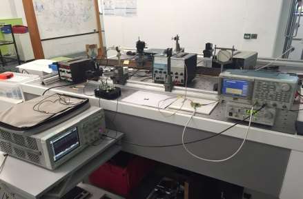
Figure 1 The Diagram of Physical Components Connection
The figure 1 above shows the components used in the system and the connection configuration of the system. First of all, the signal generator outputs data into the T junction chip (signal emitter) which includes the clock divider, prbsgen and the logic xor gate. Secondly, the data will be transmitted through the transmission channel which is made up by two vertical metal bars, one is LED light for transmitting data, the other is light sensor for receiving data. Thirdly, the data will be sent into the signal analysis and recover part which includes the shift register, pattdet and fsm components. Finally, the recovered signal and original data both will be sent into the oscilloscope to check the difference and make sure if the result is satisfied.
The objective of this project is setting up a Manchester serial data communications channel based on the vivado operation system which using System Verilog language to match this physical system. It can be used as radio channel, bit error rate tester and etc. In this project, the application of the system is designed as a bit error rate (BER) tester. As shown in figure 2 below is the design of bit error rate tester. During a complete simulation period, once received the number of errors that occurs and total number of bits that sent, then the bit error rate is available.
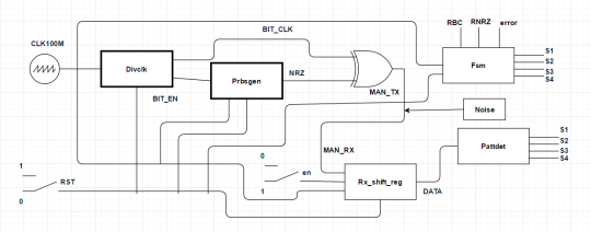
Figure 2 Bit Error Rate Tester Design
1.3 Theory
a. Bit Error Rate
Bit error rate (BER) is a key parameter that is used for transmitting digital data from one location to another in assessing systems. It is widely used to monitor the state of digital signal in different applications, such as radio data links, fibre optic data systems, Ethernet and those who transmit data through some form of networks. Generally, it affected by noise, interference and phase jitter.
Although these systems work in different ways, and have disparate impact on the bit error rate, the basics of bit error rate are still the same.
Every time when transmitting data though a data link, there is a possibility of errors being introduced into the system. If errors are introduced into the data, which means the signal will be interfered, and the system would not be integrated. So for this situation, it is necessary to assess the performance of the system, and bit error rate (BER) provides an ideal way to achieve the requirements.
Bit error rate (BER) assesses the full end to end performance of a system including the transmitter, receiver and the medium between the two. Because of this, bit error rate (BER) enables to test the actual performance of an operating system. It is different from other forms of assessment and works in a much better way.
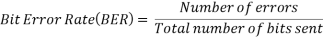
Bit error rate (BER) is defined as the rate at which errors occur in a transmission system. It can be translated into the number of errors that occur in a string of a stated number of bits directly. The definition of bit error rate in simple formula is:
If the medium between the transmitter and receiver is good and the signal to noise ratio (SNR) is high, the bit error rate will become very small, which means the error barely has noticeable effect on the overall system and could be ignored. However, if the number of errors is big, the signal to noise ratio (SNR) is low, and then the bit error rate needs to be considered. In another word, the system has been affected by noise.
Noise and the propagation path change (radio signal paths are used) are two main reasons that cause the degradation of data channel and generate the corresponding bit error rate (BER). However the two effects affect in different ways. For example the noise following a Gaussian probability function while the propagation model follow a Rayleigh model. Which means it is very necessary using statistical analysis techniques to undertake the analysis of the channel characteristics.
For fibre optic systems, bit errors usually caused by the imperfections in the components such as the optical driver, receiver, fibre and connectors that used for making the link. However it may also be introduced by optical dispersion and attenuation. What’s more, the optical receiver may detects the noise, this will also interfere the system. Typically, the fibre optical system will use sensitive photodiodes and amplifiers to respond to very small changes, and there is a possibility that high noise level will be detected.
The phase jitter that present in the system is another possible factor which enable the sampling of the data altered.
A number of factors are able to affect the bit error rate (BER). To optimize the system and acquire the required performance levels, it is very necessary to manipulate the controllable variables. Normally, in order to adjust the performance parameters at the initial design concept stages, this should be undertaken in the design stages of a data transmission system.
- Interference: The interference levels in the system are usually controlled by external factors, and can not be changed by optimizing the system design. However, the bandwidth of the system is a controllable factor. The level of interference will be reduced if the bandwidth is reduced. However the disadvantage is the achievable data throughput will be low when the bandwidth gets reduced.
- Increase transmitter power: To increase the power per bit, the power level of the system should be increased at the same time. Factors like the interference levels to other users and the impact of increasing the power output on the size of the power amplifier and overall power consumption and battery life, the impact of them should be reduced to help control the bit error rate (BER).
- Lower order modulation: Lower order modulation schemes are thinkable way to balance the bit error rate. However the achievable data throughput will reduce.
- Reduce bandwidth: Another adoptable approach is reducing the bandwidth of the system to reduce the bit error rate (BER). As a result, the system will receive lower levels of noise and the signal to noise ratio (SNR) will be improved. However, the achievable data throughput will reduce as well.
However it is not possible to achieve all the requirements, sometimes needs to do some trade-offs. In order to achieve the required bit error rate (BER), it is very necessary to balance all the available factors. When the bit error rate (BER) is lower than expected, under the risk of receiving unsatisfied levels of error correction that are introduced into the data being transmitted, further trade-offs are still necessary. Even though it may need higher levels of error correction when sending more redundant data, but the effect of any bit errors can be masked, as a result, the overall bit error rate (BER) will improve.
As radio and fibre optic system, in order to detect the indication of the performance of a data link, bit error rate (BER) is an excellent parameter for that. It is also one of the main parameter of interest in data links that detects the number of errors that occurs. Other features of the link such as the power and bandwidth, etc are able to get the performance that required after adjusting with the knowledge of the bit error rate (BER).
b. Shift Register
The Shift Register is another type of sequential logic circuit that can be used to save or transfer data in the form of binary numbers. It loads data that present on its inputs and then moves or “shifts” data to its output during every clock cycle.
Basically, a shift register is comprised by numbers of single bit “D-Type Data Latches”, one for each data bit, either a logic “0” or a “1”. The connection arrangement type is serial chain, which is able to keep turning every output from data latch become the input of the next latch.
In shift register configuration, the data bits are able to work in several ways such as fed in or out from either the left or right direction one by one or all together in parallel at the same time.
Usually, the most widely used construction of a single shift register is made up by eight individual data latches to match eight bits (one byte) data, which means the number of individual data latches is decided by the number of bits that need to be stored. While a shift register may comprise numbers of individual data latches, but all of them are driven by one common clock (CLK) signal, which makes those latches working synchronously.
Shift registers normally used in computers or calculates for storing or transferring data. The principle of it is converting data from serial to parallel or from parallel to serial format. For example, if saving data inside computer, shift registers can store all the binary numbers before them added together.
In order to set or reset the state of shift register, it always contains an additional connection with the required function. There are four different operation modes for shift register to transfer data.
- Serial-in to Serial out (SISO) – either a left or right direction, with the same clock, the data is shifted serially “IN” and “OUT” of the register one bit at a time. The figure 3 below shows an example of it which transfer data from left to right.
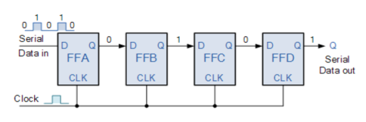
Figure 3 4-bit Serial-in to Serial-out Shift Register
- Serial-in to Parallel-out (SIPO) – one bit at a time, the data is loaded in register serially, and available to output together in parallel way. The figure 4 below shows an example of it but with 4 bits data input and output and the data transferred from left to right.
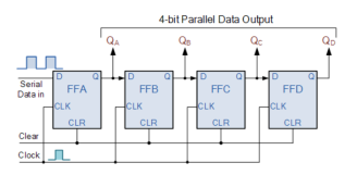
Figure 4 4-bit Serial-in to Parallel-out Shift Register
- Parallel-in to Parallel-out (PIPO) – the parallel data is introduced together into the register at the same time, and then transferred to each correspondent outputs together under the same clock pulse. The figure 5 below shows an example of it with 4 bits parallel data input and output and the direction of data movement is from left to right.
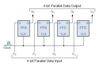
Figure 5 4-bit Parallel-in to Parallel-out Shift Register
- Parallel-in to Serial-out (PISO) – the parallel data is introduced together into the register in the meantime, and then one bit at a time, shifted out serially under the control of clock. The figure 6 below shows an example of it with 4 bits data input which transfer data from left to right.
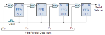
Figure 6 4-bit Parallel-in to Serial-out Shift Register
c. Pseudo Random Bit Sequence Generator (PRBSGEN)
A random bit generator is a device or algorithm that used to output a sequence of independent and unbiased binary digits in statistics. Meanwhile, a pseudo random bit sequence generator (PRBSG) is a deterministic algorithm, which means if a truly random binary sequence of length X is given, the binary sequence output of length Y >> X would be random. The input of the pseudo random bit sequence generator (PRBSG) is normally called the seed, while the output of it is called a pseudo random bit sequence. The pseudo random bit sequence generator (PRBSG) can be used as random because the value of an element of the sequence is not related to the values of any of the other elements.
However, the output of a pseudo random bit sequence generator (PRBSG) is not truly random. With all possible binary sequences of length Y, the number of possible output sequences is a small fraction maximally. After N elements, the sequence starts to repeat itself, which means it is deterministic. The aim is to receive a small truly random sequence and then expand it into a sequence with much larger length.
Generally, the implementation of pseudo random bit sequence generator (PRBSG) is based on the linear feedback shift register (LFSR). The pseudo random bit sequence generator (PRBSG) makes a sequence of logic “0” and “1” under the same probability. A sequence of serial n*(2^n -1) bits use one data pattern, and this pattern will repeat itself over time.
In the Manchester serial data communications channel, the pseudo random bit sequence generator (PRBSG) is implemented in System Verilog programming language, and used to sample two bit input data and managed through a logic xor gate, then introduce the result into the first bit of the sequence as the feedback. The output of the pseudo random bit sequence generator (PRBSG) was taken from all the nine bits of the shift register. The feedback connections of the pseudo random bit sequence generator (PRBSG) are shown in appendix A. As a result, the output of the pseudo random bit sequence generator (PRBSG) cycles between 0 to 511.
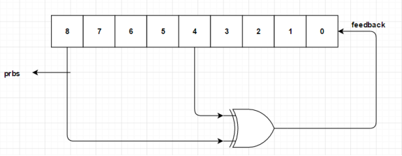
Figure 7 Principle of Pseudo Random Bit Sequence Generator (PRBSG)
d. Manchester Coding
The Manchester coding is well known because of the development in the University of Manchester. It is used to save data on the magnetic drum of the Manchester mark one computer.
In signal transmission domain, Manchester coding is widely used. However in order to achieve the same data rate but less bandwidth, the more complex codes are created such as 8B/10B encoding. Meanwhile the disadvantages of them are in the transmitter device, not able to have high tolerant of frequency errors and jitter, and receiver reference clocks. The worst problem is the Manchester encoding is not suitable for higher data rate because it will introduce some difficult frequency errors into the system. But the advantage of Manchester coding is helping recover the clock by transforming line voltage frequently, which is proportional to the clock rate directly.
It is very convenient to transmit data by media like Ethernet without a DC component because the DC component of encoded signal is not determined by the data that transmitted, which means no information will be transmitted in signal. The figure 8 below shows the principles of Manchester coding, which are:
- Each bit is transmitted once a period.
- Logic “0” expresses a low-to-high transition, logic “1” expresses a high-to-low transition.
- At the midpoint of a period, logic “0” or “1” will be interconverted.
- The transformation at the beginning of a period does not mean the data.
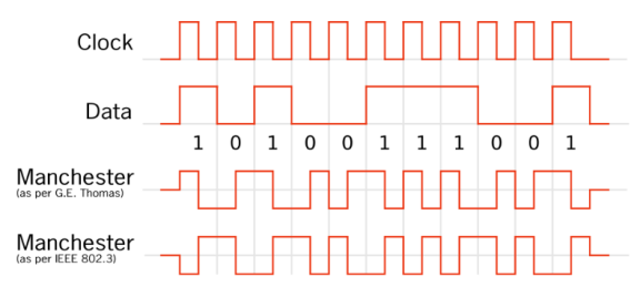
Figure 8 Principle of Manchester Encoding
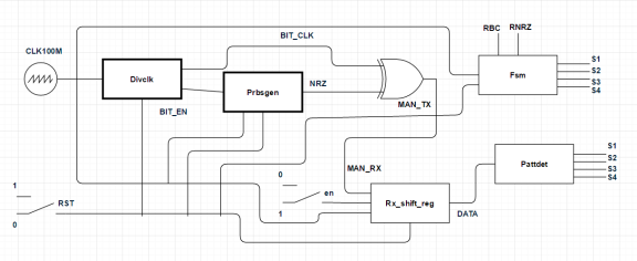
Figure 9 The Circuit Design
The figure 9 above is the complete design of whole circuit. All the components that required comprising a Manchester serial data communications channel are designed successfully. The data will be divided in the clock divider (Divclk) component, sampled in the pseudo random bit sequence generator (Prbsgen) component, and then altered into Manchester signal by a logic xor gate, through the transmission channel, the data will be sent into the shift register, combine into 10 bits DATA signal, after analysed in the Pattdet component, 4 states will be sent into finite state machine (FSM) component and be recovered as the signal of RBC and RNRZ. In this system the clock frequency is 100MHZ and the reset will set at logic “1” before the system work.
The programs of all components used in the system are shown below.
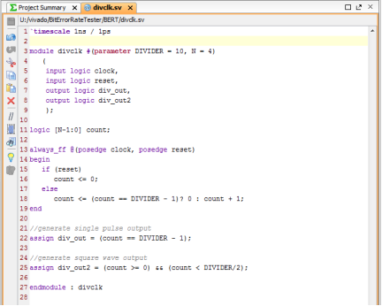
Figure 10 Clock Divider Program
The figure 10 above is the click divider program. This component is designed for dividing the clock signal into two different clock signal div_out and div_out2. These two output signals are shown in figure 13. In which the signal div_out gets one clock of high pulse every 10 clocks, the frequency is 10MHZ, and works as the specific input o the Prbsgen component. While signal div_out2 gets 5 clocks of high pluses per 5 clocks, also the frequency is 10MHZ.
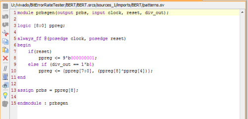
Figure 11 Prbsgen Program
The figure 11 above is the Prbsgen program. It works as a pseudo-random bit sequence generator, which records 10 bits of data each clock, when signal div_out gets high impulse, sampling the 4th and 8th data into a logic xor gate and then put the result into the 1st data position as the feedback of the sampling function. Finally, output the prbs signal (as shown in figure 7) or NRZ signal (in figure 13).
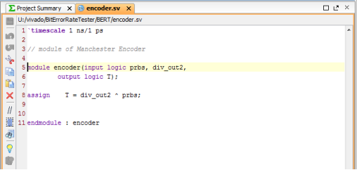
Figure 12 Logic Xor Gate Program
The figure 12 above is the logic xor gate program. In order to combine the NRZ and Bit_clk signal together and output the signal T (Manchester code) which is shown in figure 13 below. When NRZ gets high and Bit_clk gets low, output Manchester is high; when NRZ gets high and Bit_clk gets high, Manchester is low; when NRZ gets low and Bit_clk gets high, Manchester is high; when NRZ gets low and Bit_clk gets low, Manchester is low.
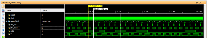
Figure 13 Manchester Signal
As the figure 13 shown, the clock divider, the pseudo random bit sequence generator (PRBSG), and logic xor gate all work well, the output signal div_out and div_out2 are both divided as required, while the prbs signal (NRZ) is as expected and the T signal (Manchester code) is the same as the signal that xors with div_out2 and prbs (NRZ) signal.
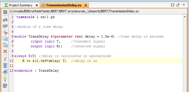
Figure 14 Transmission Delay Program
The figure 14 above is the transmission delay program. It is used to simulate the data transmission delay during the real life. Normally, errors like noise, interference and phase jitter are introduced into the data through this part, while the time of transmission delay depends on the distance between the signal emitter and receiver. In this system, the parameter of time delay set at 1.5e-6 in seconds.
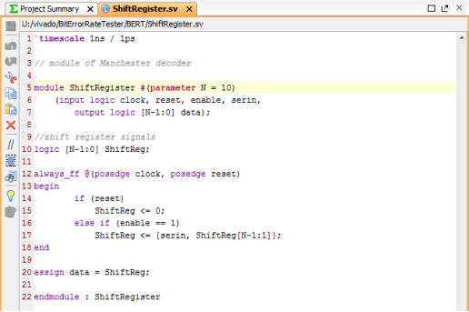
Figure 15 Shift Register Program
The figure 15 above is the signal register program. The function of it is compressing and storing the Manchester data and then transfer into pattdet component. It starts working only when reset is logic “0”, input en is logic “1”.
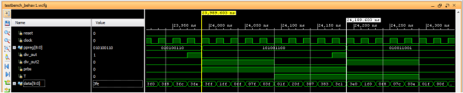
Figure 16 DATA Signal
The output of 10 bits data (DATA) is the same as required, which means the program of shift register works well.
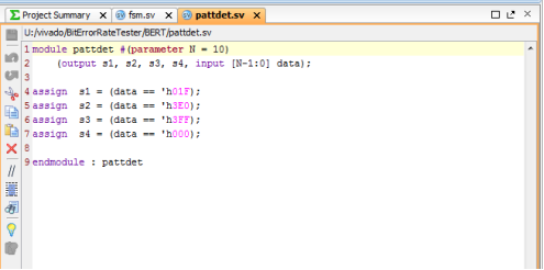
Figure 17 Pattdet Program
The figure 17 above is the pattdet program. It is used for analysing the DATA signal, and the output follows the principle which shown in table 1 below.
|
Data |
00000 00000 |
00000 11111 |
11111 00000 |
11111 11111 |
|
State |
||||
|
S1 |
10’h3EQ |
|||
|
S2 |
10’h01F |
|||
|
S3 |
10’h3FF |
|||
|
S4 |
10’h000 |
Table 1 The Working Principle of Pattdet Component
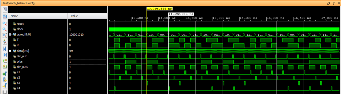
Figure 18 4 States
From figure 18 above, 4 states of s1, s2, s3, s4 are outputted separately and successfully.
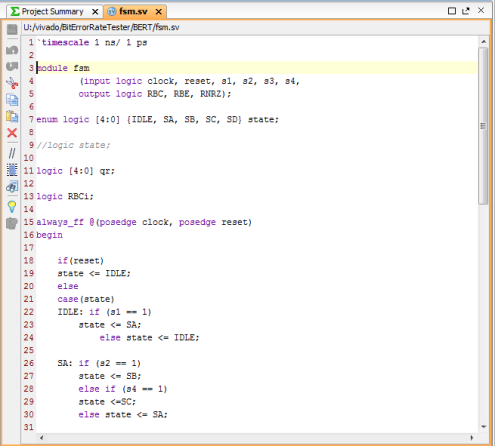
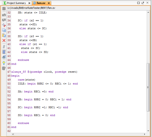
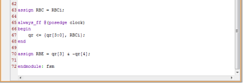
Figure 19 Finite State Machine (FSM) Program
The figure 19 above is the finite state machine (FSM) program. The function of it is analysing the 4 states and recovering the bit_clk, bit_EN and NRZ signal, and the principle of it is shown in below figure 20. From the figure 20, when signal NRZ turns to logic “0” from logic “0”, state s1 turns to s2; when signal NRZ turns to logic “1” from logic “0”, state s1 turns to s4; when signal NRZ turns to logic “1” from logic “1”, state s2 turns to s1; when signal NRZ turns to logic “0” from logic “1”, state s2 turns to s3.
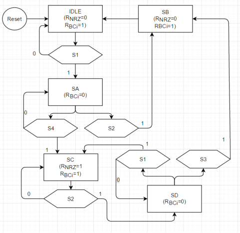
Figure 20 The Principle Of FSM
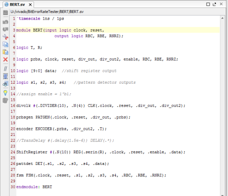
Figure 21 The Bit Error Rate Tester (BERT) Program
The figure 21 above is the catalogue program of bit error rate tester. It contains the clock divider, prbsgen, encoder (logic xor gate), shift register, pattdet and fsm program file.
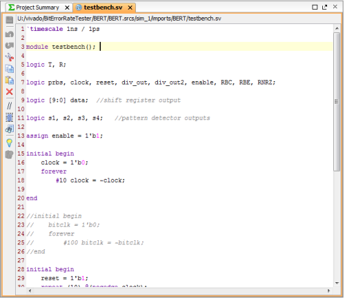
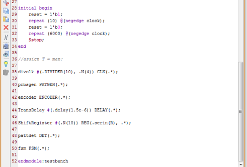
Figure 22 The Test Bench Program
The figure 22 above is the test bench program. It defines all the factors in the system and especially the period of reset and clock.
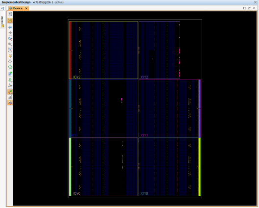
Figure 23 The Implemented Design
This is the implemented design figure, which shows the service condition of devices.
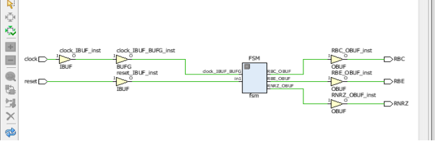
Figure 24 The Schematic Design
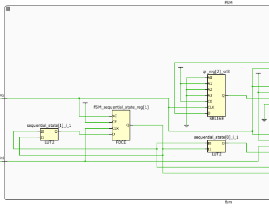
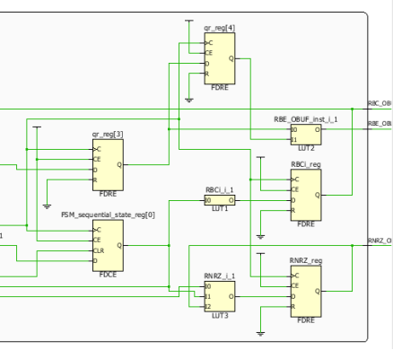
Figure 25 The Detailed Figure of FSM
The figure 25 above is the schematic design which shows the real used state of every component. However, the part of clock divider and pseudo random bit sequence generator (PRBSG) is not satisfied one. The problem may be caused by the vivado operation system software issue or the definition of clock divider and pseudo random bit sequence generator (PRBSG) is not recognised by the software.
The Manchester serial data communications channel built up successfully. In figure 26, the signal RBC, RNRZ and RBE are all recovered, just the same as the original signal bit_clk, NRZ and bit_en but with some time delay. The next objective is developing applications for the Manchester serial data communications channel. The chosen target is a bit error rate tester. By setting up a noise component for introducing random noise into the Manchester signal and then an error counter inside the finite state machine (FSM) for counting the number of errors that occurs and the total number of bits sent. As a result, the bit error rate (BER) will be able to count in the system.
Figure 26 Recovered RNRZ and RBC Signal
The figure 26 above is the final simulation result. Signal of recovered non return to zero (RNRZ), recovered bit_clock (RBC) and recovered bit_en (RBE) are all the same as their original data but with time delays.
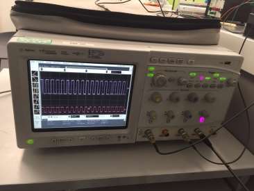
Figure 27 The Signal of Input and Recovered
From the figure 27 above, the recovered signal is almost the same as the original input data. These two figures prove the design of Manchester serial data communications channel is successful. After setting up this communication channel, the next step is developing applications for further requirements.
The theory of pseudo random bit sequence generator (PRBSG), Manchester coding, shift register and bit error rate are proved to be feasible. This project is a great opportunity to practise from research ideas to concrete systems. With the explosive growth of wireless communication system,
- Ciletti, M. (2011). ‘Advanced digital design with the Verilog HDL’. 1st ed. Boston: Prentice Hall. (Accessed: October 9 2016).
- Menezes, A., Van Oorschot, P. and Vanstone, S. (1997). ‘Handbook of applied cryptography’. 1st ed. Boca Raton: CRC Press, p.chapter. Available at: http://cacr.uwaterloo.ca/hac/about/chap5.pdf (Accessed: December 25 2016).
- MUKHERJEE, S. and PANDEY, R. (2007). ‘DESIGN AND IMPLEMENTATION OF PRBS GENERATOR USING VHDL’. bachelor. Department of Electronics & Communication Engineering National Institute of Technology Rourkela. Available at: https://pdfs.semanticscholar.org/42e7/490ec8905ea8afe618c6882f2b050ece2ae4.pdf (Accessed: October 14 2016).
- Malviya, S. and Kumari, P. (2014). ‘Implementation of Pseudo-Noise Sequence Generator on FPGA Using Verilog’. [online] Dept of Electronics and Communication, Sobhasaria Group of Institution, Sikar, Rajasthan. Available at: https://www.ripublication.com/irph/ijeee_spl/ijeeev7n8_16.pdf [Accessed
Cite This Work
To export a reference to this article please select a referencing stye below:
Related Services
View all


DMCA / Removal Request
If you are the original writer of this essay and no longer wish to have your work published on UKEssays.com then please click the following link to email our support team:
Request essay removal