Ration Materials Distribution based on GSM and RFID Technology
Info: 21348 words (85 pages) Dissertation
Published: 13th Dec 2019
Tagged: TechnologyBuilding Materials
CHAPTER 1
INTRODUCTION
Public Distribution System is government administered chain of shops which distributes groceries at subsidized rates. There are about 5,00,000 ration shops across India. In India over 54 crore people are getting benefited by public distribution system. The major groceries distributed are rice, wheat, kerosene, sugar etc. Its greatest achievement lies in preventing famines in India.
The objectives of Public Distribution System are:
- To provide groceries at low prices to the vulnerable sections of the society.
- To influence the price of groceries in open market.
| S.No. | Item Name | Actual Price(per kg/ltr) | SubsidizedPrice( kg/ltr) |
| 1 | Rice | 20 | 1 |
| 2 | Wheat | 40 | 7 |
| 3 | Kerosene | 38 | 19 |
| 4 | Sugar | 42 | 13.50 |
Ration card is an official document entitling the owner to a ration of groceries. One card per family is issued by the state government for people under poverty line. People having ration card can buy the groceries from ration shop for subsidized rates fixed by the Government. In the ration shop, first we need to submit the ration card and then it is authenticated. Then they will issue the quantity of groceries eligible through weighting system manually. Then they will record the details. But this system is having two draw backs, first one is chance of forgery and second no transparency to customers.
In this project, we propose ration materials distribution based on GSM and RFID Technology to avoid the drawbacks. Radio-frequency identification (RFID) based access control system allows only authorized or responsible persons to get the materials from ration shops. RFID card acts as ration card and stores the name and phone number of the customer and can avoid forgery and theft. GSM is used to communicate the information with cardholders to provide transparency.
1.1. Objective
- The objective of the designed system is to provide transparency and avoid forgery in ration shops.
- Forgery can be avoided by Radio Frequency Identification (RFID) technology which replaces conventional ration cards by RFID tags .
- The microcontroller sends the information to customer using Global System for Mobile (GSM) technology which would create transparency in the system.
1.2. Literature Survey
The existing predictable ration system has the basic issues of renewing the ration card every year by the employees to the malpractices done by the ration store dealers like diverting food grains to open market to make profit. To tackle this problems K.Balakarthik proposed the “Cloud-Based Ration Card System using RFID and GSM Technology” [1], presents an efficient method for the user to buy the products in the ration shop by just irregular the card at the RFID reader. The user authentication is done by sending a random password text to the user mobile which has to be entered in a keypad. The purchase is validated by the employee only after the details are entered in a windows application which stores the user’s personal and purchase information. The current PDS involves corruption and illegal smuggling of goods because of manual work. A.N. Maduretal Developed the “Automation in Rationing System using Arm 7” [2], S.Valarmathy et.al. Proposed the “Automatic Ration Material Distributions Based on GSM and RFID”[3]. Here each customer is provided with RFID cards. In this system, first user is authenticated, and then system shows the balance of person. User have to enter the amount of Kg he want to withdraw. If the user will have sufficient balance to withdraw the current amount, system will open the valve. Through valve grain will come and it will get weighted by weight sensor. Once the count reached the entered amount controller automatically shut down the valve and updates the account of the customer. The updated account information is send to the customer’s mobile using GSM. Rationing distribution is one of the widely provocative issue that involves wrong entries in stock register of shop containing wrong stock information of the products that is supplied to the public, so Rajesh C. Pingle et.al. Suggested the “Automatic Rationing for Public Distribution System (PDS) using RFID and GSM Module to Prevent Irregularities” [4], in this automated system conventional ration card is replaced by smartcard in which all the details about users are provided including their AADHAR number which is used for user authentication. To involve government in the process we proposed connecting the system at ration shop to a central database (provided by government.) via GSM and RS232. Hence it is possible to prevent the corruption and irregularities at ration shop. The existing PDS system causes congestion at ration shop due to manual work so S. Sukhumar et.al. Proposed the “Automatic Rationing System Using Embedded System Technology” [5], in this the ration distribution system is automated by using PLC. This automated ration system replaces the conventional ration card system by smart card. The proposed ration shop system is connected to the government database via GSM modules, which further sends the up-to-date information to the government and the consumer. So we suggested the “e– Ration Shop: An Automation Tool for Fair Price Shop under the Public Distribution System”.
1.3. Existing System
India’s Public Distribution System (PDS) is the largest distribution network in the world. The responsibility of distributing food grains lies with the government. The major groceries distributed are rice, wheat, kerosene….etc. The main objective of Public distribution system is to provide groceries at low prices to the vulnerable sections of the society and to influence the price of groceries in open market. Public Distribution System (PDS) faces the challenges like quality of food grains and inaccurate identification of ration card holders. In the existing system one ration card per family is issued by the state government for people under poverty line. Ration card holders will buy the groceries from ration shop for subsidized rates fixed by the Government .Each family under poverty line is eligible for 15 kg of food grains. In the ration shop, first we need to submit the ration card and then it is authenticated. Then they will issue the quantity of groceries eligible through weighting system manually. Then they will record the details. This method is inaccurate, tedious and may sometimes result to malpractices.
1.4. Scope Of Work
RFID tag replaces the ration cards in this project. We are storing the name and phone number of the customer in the rfid tag. Due to low memory of microcontroller details of only three customers are stored. When the tag is read by the rfid reader name and phone number of the person is displayed on the LCD screen. Then the required product and quantity has to be given through keypad. Immediately a message is sent to the customer through GSM.
We can store all the details of the customer like aadhar number, annual income, family details etc in the tags. Because of the memory constraint of microcontroller, we are having only three ration card holders. This memory constraint can be eliminated by using servers having large memory to store customer’s information. When there is shortage of groceries at ration shop immediately information can be sent to authorities by short message service. We can also create a website to display the details of customers and the groceries they took.
1.5 Organisation Of Report
This report contains seven chapters. They are introduction, overview of embedded system, hardware details, software tools, software implementation and conclusion.
Chapter 1-This chapter includes introduction to the project, objective, literature survey, existing system and scope of work
Chapter 2-Brief view of embedded system, overview of embedded architecture and it’s applications are discussed in this chapter.
Chapter 3-In this chapter block diagram, design issues and brief discussion about hardware components are discussed.
Chapter 4-This chapter includes the implementation of keil software and the proload software .
Chapter 5-In this chapter the schematic diagram and flow chart of the project are discussed.
Chapter 6-The implementation results and advantages of the project are discussed in this chapter.
Chapter 7-In this chapter the conclusion and future scope are discussed.
CHAPTER 2
OVERVIEW OF EMBEDDED SYSTEMS
2.1. Introduction
An embedded system can be defined as a computing device that does a specific focused job. Appliances such as the air-conditioner, VCD player, DVD player, printer, fax machine, mobile phone etc. are examples of embedded systems. Each of these appliances will have a processor and special hardware to meet the specific requirement of the application along with the embedded software that is executed by the processor for meeting that specific requirement. The embedded software is also called “firm ware”. The desktop/laptop computer is a general purpose computer. You can use it for a variety of applications such as playing games, accounting, software development and so on. In contrast, the software in the embedded systems is always fixed listed below:
Embedded systems do a very specific task, they cannot be programmed to do different things. Embedded systems have very limited resources, particularly the memory. Generally, they do not have secondary storage devices such as the CDROM or the floppy disk. Embedded systems have to work against some deadlines. A specific job has to be completed within a specific time. In some embedded systems, called real-time systems, the deadlines are stringent. Missing a deadline may cause a catastrophe-loss of life or damage to property. Embedded systems are constrained for power. As many embedded systems operate through a battery, the power consumption has to be very low.
Some embedded systems have to operate in extreme environmental conditions such as very high temperatures and humidity.
2.2. Embedded System Architecture
Each embedded system comprises of custom-manufactured equipment worked around a Central Processing Unit (CPU). This equipment likewise contains memory chips onto which the product is stacked. The product dwelling on the memory chip is likewise called the ‘firmware’. The implanted framework design can be spoken to as a layered engineering as appeared in Fig 2.1.
Application software
Operating system
Hardware
Fig 2.1-Embedded layer architecture
The embedded system continues running over the hardware, and the application programming continues running over the embedded system. A comparable outline is correlated to any PC including a desktop PC. Regardless, there are colossal complexities. It is not important to have a working framework in each installed framework. For little mechanical assemblies, for instance, remote control units, air circulation and cooling frameworks, toys et cetera, there is no prerequisite for a working framework and you can create only the item specific to that application. For applications including complex setting it up, is reasonable to have a working framework. In such a case, you need to organize the application programming with the working framework and a short time later trade the entire programming on to the memory chip. Once the item is traded to the memory chip, the item will continue running for a long time you don’t need to reload new programming.
By and by, let us see the purposes of enthusiasm of the distinctive building bits of the gear of an embedded structure. As showed up in Fig2.2 the building squares appear to be
- Central Processing Unit (CPU)
- Memory (Read-only Memory and Random Access Memory)
- Input Devices
- Output devices
- Communication interfaces
- Application-specific circuitry


Read only memory(ROM)
Random Access Memory(RAM)
Output Devices


Central Processing Unit(CPU)
Input Devices
Application Specific circuitry

Communication interfaces
Figure 2.2: Embedded Architecture
A.Central Processing Unit (CPU):
The Central Processing Unit (processor, in short) can be any of the accompanying: microcontroller, microchip or Digital Signal Processor (DSP). A smaller scale controller is an ease processor. Its principle fascination is that on the chip itself, there will be numerous different segments, for example, memory, serial correspondence interface, simple to computerized converter and so on. In this way, for little applications, a smaller scale controller is the best decision as the quantity of outside parts required will be less. Then again, microchips are all the more capable, yet you have to utilize numerous outer segments with them. D5P is utilized for the most part for applications in which flag handling is included, for example, sound and video preparing.
B. Memory:
The memory is categorized as Random Access 11emory (RAM) and Read Only Memory (ROM). The contents of the RAM will be erased if power is switched off to the chip, whereas ROM retains the contents even if the power is switched off. So, the firmware is stored in the ROM. When power is switched on, the processor reads the ROM; the program is program is executed.
C. Input devices:
Not at all like the desktops, the input devices to an embedded system have extremely restricted ability. There will be no console or a mouse, and subsequently collaborating with the implanted framework is no simple undertaking. Many inserted frameworks will have a little keypad-you squeeze one key to give a particular summon. A keypad might be utilized to enter just the digits. Many inserted frameworks utilized as a part of process control don’t have any information gadget for client association; they take contributions from sensors or transducers 1’fnd deliver electrical signs that are thus bolstered to different frameworks.
D. Output devices:
The output devices of the embedded system additionally have exceptionally constrained ability. Some embedded systems will have a Light Emitting Diodes (LEDs) to demonstrate the wellbeing status of the framework modules, or for visual sign of alerts. A little Liquid Crystal Display (LCD) may likewise be utilized to show some essential parameters.
E. Communication interfaces:
The embedded systems may need to, interact with other embedded systems at they may have to transmit data to a desktop. To facilitate this, the embedded systems are provided with one or a few communication interfaces such as RS232, RS422, RS485, Universal Serial Bus (USB), IEEE 1394, Ethernet etc.
F. Application-specific circuitry:
Sensors, transducers, extraordinary handling and control hardware might be required fat an implanted framework, contingent upon its application. This hardware connects with the processor to do the fundamental work. The whole equipment must be given power supply either through the 230 volts principle supply or through a battery. The equipment needs to plan such that the power utilization is limited.
2.3. Application Areas
Almost 99 for each penny of the processors made wind up in installed frameworks. The installed framework market is one of the most noteworthy development ranges as these frameworks are utilized as a part of exceptionally market fragment customer hardware, office mechanization, modern robotization, biomedical building, remote correspondence, information correspondence, broadcast communications, transportation, military et cetera.
Consumer appliances: At home we use a number of embedded systems which include digital camera, digital diary, DVD player, electronic toys, microwave oven, remote controls for TV and air-conditioner, VCO player, video game consoles, video recorders etc. Today’s high-tech car has about 20 embedded systems for transmission control, engine spark control, air-conditioning, navigation etc. Even wristwatches are now becoming embedded systems. The palmtops are powerful embedded systems using which we can carry out many general-purpose tasks such as playing games and word processing.
Office automation: The office automation products using embedded systems are copying machine, fax machine, key telephone, modem, printer, scanner etc. This has made the work more easier in the offices.
Industrial automation: Today a considerable measure of businesses utilize implanted frameworks for process control. These incorporate pharmaceutical, bond, sugar, oil investigation, atomic vitality, power era and transmission. The installed frameworks for modern utilize are intended to complete particular undertakings, for example, observing the temperature, weight, moistness, voltage, current and so on., and after that make proper move in view of the checked levels to control different gadgets or to send data to an incorporated observing station. In perilous mechanical condition, where human nearness must be maintained a strategic distance from, robots are utilized, which are customized to do particular occupations. The robots are presently winding up plainly effective and do many intriguing and muddled errands, for example, equipment get together.
Medical electronics: Practically every therapeutic gear in the doctor’s facility is an inserted framework. These types of gear incorporate analytic guides, for example, ECG, EEG, pulse measuring gadgets, X-beam scanners; hardware utilized as a part of blood examination, radiation, colonscopy, endoscopy and so on. Improvements in therapeutic gadgets have cleared route for more precise analysis of ailments.
Computer networking: PC organizing items, for example, spans, switches, Integrated Services Digital Networks (ISDN), Asynchronous Transfer Mode (ATM), X.25 and outline hand-off switches are inserted frameworks which actualize the vital information correspondence conventions. For instance, a switch interconnects two systems. The two systems might run distinctive convention stacks. The switch’s capacity is to acquire the information bundles from approaching pores, dissect the parcels and send them towards the goal in the wake of doing essential convention change. Most systems administration types of gear, other than the end frameworks (desktop PCs) we use to get to the systems, are installed frameworks.
Telecommunications: In the field of broadcast communications, the implanted frameworks can be arranged as supporter terminals and system gear. The supporter terminals, for example, key phones, ISDN telephones, terminal connectors, web cameras are implanted frameworks. The system gear incorporates multiplexers, different get to frameworks, Packet Assemblers Dissemblers (PADs), sate11ite modems and so forth. IP telephone, IP passage, IP guardian and so on are the most recent installed frameworks that give minimal effort voice correspondence over the Internet.
Wireless technologies: Propels in portable correspondences are clearing path for some fascinating applications utilizing installed frameworks. The cell phone is one of the wonders of the most recent decade of the 20’h century. It is an intense inserted framework that gives voice correspondence while we are moving. The Personal Digital Assistants and the palmtops can now be utilized to get to interactive media benefits over the Internet. Portable correspondence framework, for example, base station controllers, versatile exchanging focuses are additionally effective inserted frameworks.
Insemination: Testing and estimation are the essential prerequisites in all logical and building exercises. The measuring hardware we use in research centers to quantify parameters, for example, weight, temperature, weight, stickiness, voltage, ebb and flow and so on are altogether installed frameworks. Test gear, for example, oscilloscope, range analyzer, rationale analyzer, convention analyzer, radio correspondence test set and so forth are installed frameworks worked around capable processors. Thank to scaling down, the test and measuring hardware are currently getting to be noticeably compact encouraging simple testing and estimation in the field by field-work force.
Security: Security of people and data has dependably been a noteworthy issue. We have to secure our homes and workplaces; and furthermore the data we transmit and store. Creating installed frameworks for security applications is a standout amongst the most lucrative organizations these days. Security gadgets at homes, workplaces, air terminals and so on for validation and confirmation are implanted frameworks. Encryption gadgets are about 99 for every penny of the processors that are fabricated wind up in~ implanted frameworks. Inserted frameworks discover applications in. each modern portion buyer gadgets, transportation, flying, biomedical building, fabricating, prepare control and mechanical mechanization, information correspondence, media transmission, resistance, security and so on.Used to scramble the information/voice being transmitted on correspondence connections, for example, phone lines. Biometric frameworks utilizing unique mark and face acknowledgment are currently being broadly utilized for client confirmation in keeping money applications and in addition for get to control in high security structures.
Finance: Monetary managing through money and checks are presently gradually clearing path for exchanges utilizing shrewd cards and ATM (Automatic Teller Machine, additionally extended as Any Time Money) machines. Shrewd card, of the measure of a Visa, has a little smaller scale controller and memory; and it interfaces with the keen card peruser! ATM machine and goes about as an electronic wallet. Shrewd card innovation has the capacity of introducing a cashless society. Indeed, the rundown goes on. It is no misrepresentation to state that eyes wherever you go, you can see, or possibly feel, the work of an implanted framework!
CHAPTER 3
HARDWARE DETAILS
This chapter briefly explains about the Hardware components of the project. It discusses the design and working of the design with the help of block diagram in detail. It explains the features, timer programming, serial communication, interrupts of 8052 microcontroller. It also explains the various modules used in this project.
3.1 Project Design
The execution of the venture configuration can be partitioned in two sections.
- Hardware usage
- Firmware usage
Hardware utilization deals in drawing the schematic on the plane paper according to the application, testing the schematic blueprint over the breadboard using the diverse IC’s to find if the diagram meets the objective, doing the PCB configuration of the schematic attempted on breadboard, finally setting up the heap up and testing the made gear.
The firmware part deals in programming the microcontroller with the objective that it can control the operation of the IC’s used as a piece of the execution. In the present work, we have used the Orcad layout programming for PCB circuit arrange, the Keil µv3 programming change gadget to create and total the source code, which has been made in the C vernacular. The Proload programming engineer has been used to make this join code into the microcontroller. The firmware utilization is cleared up in the accompanying segment.
The wander plan and rule are cleared up in this part using the piece outline and circuit chart. The square blueprint discusses the required parts of the arrangement and working condition is cleared up using circuit diagram and system wiring graph.
A. Hardware Design Issues
Microcontroller (8052)
The 8052 microcontroller has a internal RAM of 256 bytes whereas the 8051 has 128 bytes which is required to store the code of the project. The 8052 microcontroller has an internal memory of 8 kb which is required to store the details of the ration card holders. We can have other microcontrollers with same memory but 8052 is cost effective. The input/output pins of the microcontroller suits the requirement of the project. The two interrupts, one tx , one rx pins are enough for supporting GSM and RFID.
Keypad
We are using 4*3 keypad .We are selecting the grocery by the option and the weight is to be entered in the number of kilograms. So, we need only numeric keypad and that is the reason we are going for an 4*3 keypad.
LCD
A 16*2 LCD display is very basic module and is preferred over other multi segment displays and LED displays. The reasons being the LCD is economical, easily programmable and have no limitation of displaying special characters. We are using 16*2 LCD because we need to display the name and the phone number of the card holder.
RFID Module
We are using an EM-18 RFID reader whose frequency is 125 KHz .We are using the module with this frequency to achieve our purpose of contactless proximity reading .We can even have long distance reliable reading with high frequency which is not cost effective. This module is widely used in embedded systems for security purpose.
GSM Module
We need a GSM module to send SMS in our project. We are using SIM900 GSM modem over SIM300 because it is a quad band modem which operates in different frequency bands and offers improved GPRS functionalities.
B. Block Diagram of the Project and its Description
The block diagram of the design is as shown in Fig 3.1. It consists of power supply unit, microcontroller, GSM, keypad, RFID and MAX232 and LCD. The brief description of each unit is explained as follows.
Block diagram
µC
KEY PAD


LCD DISPLAY
POWERSUPPLY


RFID READER

GSM MODULE
Figure 3.1: Block Diagram
3.2 Power Supply
The contribution to the circuit is connected from the controlled power supply appeared in figure 3.2. The A.C. input i.e., 230V from the mains supply is venture around the transformer to 12V and is bolstered to a rectifier. The yield acquired from the rectifier is a throbbing D.C voltage. So with a specific end goal to get an unadulterated D.C voltage, the yield voltage from the rectifier is nourished to a channel to expel any A.C segments show even after amendment. Presently, this voltage is given to a voltage controller to acquire an unadulterated consistent dc voltage.
In our venture control supply necessity is to work whole framework. Each electronic gadget is worked utilizing power supply just or put away supply like batteries. However, utilizing batteries is financially savvy yet control supply unit gives ceaseless supply from mains. So it is shoddy one contrasted with batteries.


 Vmsinωt


 Iout
Iout
Regulator
Transformer
Rectifier
Filter
load
 To AC line
Vout


Figure 3.2: Components of a regulated power supply
A.Transformer
As a rule, DC voltages are required to work different electronic hardware and these voltages are 5V, 9V or 12V. Be that as it may, these voltages can’t be gotten straightforwardly. Consequently the a.c input accessible at the mains supply i.e., 230V is to be conveyed down to the required voltage level. This is finished by a transformer. In this manner, a stage down transformer is utilized to diminish the voltage to a required level.
B. Rectifier
The yield from the transformer is encouraged to the rectifier. It changes over A.C. into throbbing D.C. The rectifier might be a half wave or a full wave rectifier. In this venture, an extension rectifier is utilized as a result of its benefits like great strength and full wave correction.
C. Channel
Capacitive channel is utilized as a part of this venture. It expels the swells from the yield of rectifier and smoothens the D.C. Yield got from this channel is consistent until the mains voltage and load is looked after steady. Be that as it may, if both of the two is differed, D.C. voltage got now changes. Accordingly a controller is connected at the yield organize.
D. Voltage controller:
As the name itself infers, it controls the info connected to it. A voltage controller is an electrical controller intended to consequently keep up a steady voltage level. In this venture, control supply of 5V and 12V are required. So as to acquire these voltage levels 7805 and 7812 voltage controllers are to be utilized. The primary number 78 speaks to positive supply and the numbers 05, 12 speak to the required yield voltage levels.


 3.3. Microcontroller (8052)
Microchips and microcontrollers are generally utilized as a part of installed frameworks items. Microcontroller is a programmable gadget. A microcontroller has a CPU notwithstanding a settled measure of RAM, ROM, I/O ports and a clock installed all on a solitary chip. The settled measure of on-chip ROM, RAM and number of I/O ports in microcontrollers makes them perfect for some applications in which cost and space are basic.
The Intel 8052 is Harvard engineering, single chip microcontroller (µC) which was created by Intel in 1980 for use in implanted frameworks. It was well known in the 1980s and mid 1990s, however today it has to a great extent been superseded by an unfathomable scope of improved gadgets with 8051-good processor centers that are fabricated by more than 20 autonomous makers including Atmel, Infineon Technologies and Maxim Integrated Products.
8052 is a 8-bit processor, implying that the CPU can take a shot at just 8 bits of information at once. Information bigger than 8 bits must be broken into 8-bit pieces to be handled by the CPU. 8052 is accessible in various memory sorts, for example, UV-EPROM, Flash and NV-RAM.
Features of AT89S52
• 8K Bytes of Re-programmable Flash Memory.
• RAM is 256 bytes.
• 4.0 V to 5.5 Operating Range.
• Fully Static Operation: 0 Hz to 33 MHz’s
• Three-level Program Memory Lock.
• 256 x 8-bit Internal RAM.
• 32 Programmable I/O Lines.
• Three 16-bit Timer/Counters.
• Eight Interrupt Sources.
• Full Duplex UART Serial Channel.
• Low-power Idle and Power-down Modes.
• Interrupt recovery from power down mode.
• Watchdog timer.
• Dual data pointer.
• Power-off flag.
• Fast programming time.
• Flexible ISP programming (byte and page mode).
Description
The AT89s52 is a low-voltage, prevalent CMOS 8-bit microcomputer with 8K bytes of Flash programmable memory. The device is made using Atmel’s high thickness nonvolatile memory advancement and is impeccable with the business standard MCS-51 rule set. The on chip streak allows the program memory to be rethought in structure or by a standard non erratic memory programming engineer. By joining a versatile 8-bit CPU with Flash on a strong chip, the Atmel AT89s52 is an exceptional microcomputer, which gives an exceedingly versatile and monetarily wise response for some embedded control applications.
Also, the AT89s52 is arranged with static basis for operation down to zero repeat and sponsorships two programming selectable power saving modes. The Idle Mode stops the CPU while allowing the RAM, clock/counters, serial port and meddle with system to continue working. The close down mode saves the RAM substance yet sets the oscillator crippling all other chip limits until the accompanying hardware reset.
Pin diagram:
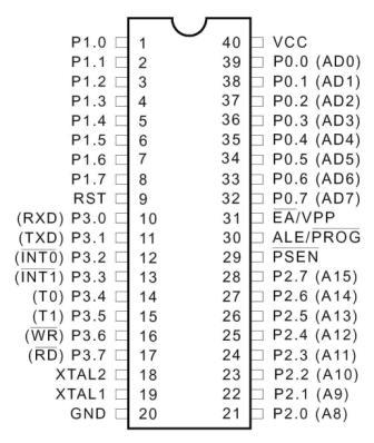
Figure 3.3: Pin Diagram of 8052
Pin description
Vcc Pin 40 provides supply voltage to the chip. The voltage source is +5V.
GND Pin 20 is the ground.
Port 0
Port 0 is a 8-bit open deplete bidirectional I/O port. As a yield port, each stick can sink eight TTL inputs. At the point when 1s are composed to port 0 sticks, the pins can be utilized as high impedance inputs. Port 0 can likewise be arranged to be the multiplexed low-arrange address/information transport amid gets to outer program and information memory. In this mode, P0 has inner draw ups.
Port 0 likewise gets the code bytes amid Flash programming and yields the code bytes amid Program check. Outer draw ups are required amid program check.
Port 1
Port 1 is a 8-bit bidirectional I/O port with inside draw ups. The Port 1 yield backings can sink/source four TTL inputs. Right when 1s are created to Port 1 pins, they are pulled high by within draw ups and can be used as information sources. As information sources, Port 1 sticks that are remotely being pulled low will source current (IIL) because of the internal draw ups. In addition, P1.0 and P1.1 can be organized to be the clock/counter 2 external number data (P1.0/T2) and the clock/counter 2 trigger data (P1.1/T2EX), independently, as showed up in the going with table.
Port 1 also gets the low-orchestrate address bytes in the midst of Flash programming and check.
Port 2
Port 2 is a 8-bit bidirectional I/O port with inside drive ups. The Port 2 yield supports can sink/source four TTL inputs. Right when 1s are created to Port 2 pins, they are pulled high by the internal drive ups and can be used as data sources. As information sources, Port 2 sticks that are remotely being pulled low will source current (IIL) because of within constrain ups.
Port 2 transmits the high-mastermind address byte in the midst of brings from outside program memory and in the midst of gets to external data memory that usages 16-bit addresses (MOVX @ DPTR). In this application, Port 2 uses strong inside constrain ups while emanating 1s. In the midst of gets to external data memory that usages 8-bit addresses (MOVX @ RI), Port 2 transmits the substance of the P2 Special Function Register. The port moreover gets the high-orchestrate address bits and some control signals in the midst of Flash programming and affirmation.
Port 3
Port 3 is a 8-bit bidirectional I/O port with inward drive ups. The Port 3 yield backings can sink/source four TTL inputs. Right when 1s are formed to Port 3 pins, they are pulled high by the inside draw ups and can be used as wellsprings of data. As data sources, Port 3 sticks that are remotely being pulled low will source current (IIL) in light of the constrain ups. Port 3 gains some power signals for Flash programming and check.
Port 3 in like manner serves the components of various extraordinary components of the AT89S52, as showed up in the going with table.
RST
Reset input A high on this stick for two machine cycles while the oscillator is running resets the gadget. This stick drives high for 98 oscillator periods after the Watchdog times out. The DISRTO bit in SFR AUXR (address 8EH) can be utilized to handicap this component. In the default condition of bit DISRTO, the RESET HIGH out element is empowered.
Lager/PROG
Address Latch Enable (ALE) is a yield beat for locking the low byte of the convey in the midst of gets to outside memory. This stick is in like manner the program beat input (PROG) in the midst of Flash programming.
In average operation, ALE is released at a relentless rate of 1/6 the oscillator repeat and may be used for outside arranging or timing purposes. Note, regardless, that one ALE pulse is skipped in the midst of each passage to external data memory.
In case pined for, ALE operation can be crippled by setting bit 0 of SFR region 8EH. With the bit set, ALE is changing just in the midst of a MOVX or MOVC rule. Something else, the stick is sadly pulled high. Setting the ALE-cripple bit has no effect if the microcontroller is in external execution mode.
PSEN
Program Store Enable (PSEN) is the perused strobe to outside program memory. At the point when the AT89S52 is executing code from outer program memory, PSEN is actuated twice each machine cycle, aside from that two PSEN enactments are skipped amid each entrance to outside information memory.
EA/VPP
Outer Access Enable EA must be strapped to GND keeping in mind the end goal to empower the gadget to bring code from outside program memory areas beginning at 0000H up to FFFFH. Note, be that as it may, that if bolt bit 1 is customized, EA will be inside hooked on reset.
EA ought to be strapped to VCC for inner program executions. This stick likewise gets the 12-volt programming empower voltage (VPP) amid Flash programming.
XTAL1
Contribution to the altering oscillator intensifier and contribution to the inside clock working circuit.
XTAL2
Output from the altering oscillator speaker
XTAL1 and XTAL2 are the information and yield, independently, of a changing intensifier that can be intended for use as an on-chip oscillator. Either a quartz valuable stone or ceramic resonator may be used. To drive the device from an outside clock source, XTAL2 should be left isolates while XTAL1 is driven. There are no necessities on the commitment cycle of the external clock movement, since the commitment to the internal planning equipment is through a detachment by-two flip-droop, however slightest and most outrageous voltage high and low time conclusions must be viewed.
Uncommon Function Registers
A guide of the on-chip memory range called the Special Function Register (SFR) space is appeared in the accompanying table.
It ought to be noticed that not the majority of the locations are involved and abandoned locations may not be executed on the chip. Perused gets to these locations will when all is said in done return irregular information, and compose gets to will have an uncertain impact.
Client programming ought not compose 1s to these unlisted areas, since they might be utilized as a part of future items to summon new components. All things considered, the reset or idle estimations of the new bits will dependably be 0.
Clock 2 Registers
Control and status bits are contained in registers T2CON and T2MOD for Timer 2. The enroll combine (RCAP2H, RCAP2L) is the Capture/Reload enlist for Timer 2 in 16-bit catch mode or 16-bit auto-reload mode.
Interfere with Registers
The individual hinder empower bits are in the IE enroll. Two needs can be set for each of the six intrude on sources in the IP enroll.
Double Data Pointer Registers
To encourage getting to both interior and outer information memory, two banks of 16-bit Data Pointer Registers are given: DP0 at SFR address areas 82H-83H and DP1 at 84H and 85H. Bit DPS = 0 in SFR AUXR1 chooses DP0 and DPS = 1 chooses DP1. The client ought to ALWAYS introduce the DPS bit to the proper incentive before getting to the separate Data Pointer Register.
Control off Flag
The Power off Flag (POF) is situated at bit 4 (PCON.4) in the PCON SFR. POF is set to “1” amid catalyst. It can be set and rest under programming control and is not influenced by reset.
Memory Organization
MCS-51 gadgets have a different address space for Program and Data Memory. Up to 64K bytes each of outside Program and Data Memory can be tended to.
Program Memory
On the off chance that the EA stick is associated with GND, all program brings are coordinated to outer memory. On the AT89S52, if EA is associated with VCC, program gets to addresses 0000H through 1FFFH are coordinated to inner memory and gets to addresses 2000H through FFFFH are to outer memory.
Data Memory
The AT89S52 actualizes 256 bytes of on-chip RAM. The upper 128 bytes possess a parallel deliver space to the Special Function Registers. This implies the upper 128 bytes have an indistinguishable locations from the SFR space yet are physically separate from SFR space.
At the point when a direction gets to an inward area above address 7FH, the address mode utilized as a part of the guideline indicates whether the CPU gets to the upper 128 bytes of RAM or the SFR space. Guidelines which utilize coordinate tending to get to the SFR space.
For instance, the accompanying direct tending to guideline gets to the SFR at area 0A0H (which is P2).
MOV 0A0H, #data
The guidelines that utilization circuitous tending to get to the upper 128 bytes of RAM. For instance, the accompanying aberrant tending to direction, where R0 contains 0A0H, gets to the information byte at address 0A0H, as opposed to P2 (whose address is 0A0H).
MOV @R0, #data
It ought to be noticed that stack operations are cases of roundabout tending to, so the upper 128 bytes of information RAM are accessible as stack space.
Guard dog Timer (One-time Enabled with Reset-out)
The WDT is planned as a recuperation strategy in circumstances where the CPU might be subjected to programming upsets. The WDT comprises of a 14-bit counter and the Watchdog Timer Reset (WDTRST) SFR. The WDT is defaulted to debilitate from leaving reset. To empower the WDT, a client must compose 01EH and 0E1H in grouping to the WDTRST enroll (SFR area 0A6H).
At the point when the WDT is empowered, it will increase each machine cycle while the oscillator is running. The WDT timeout period is subject to the outside clock recurrence. There is no real way to debilitate the WDT with the exception of through reset (either equipment reset or WDT flood reset). At the point when WDT floods, it will drive a yield RESET HIGH heartbeat at the RST stick.
UART
The Atmel 8052 Microcontrollers execute three universally useful, 16-bit clocks/counters. They are distinguished as Timer 0, Timer 1 and Timer 2 and can be autonomously designed to work in an assortment of modes as a clock or as an occasion counter. When working as a clock, the clock/counter keeps running for a customized time allotment and after that issues an intrude on demand. When working as a counter, the clock/counter tallies negative moves on an outside stick. After a preset number of tallies, the counter issues an intrude on demand. The different working methods of every clock/counter are depicted in the accompanying segments.
A fundamental operation comprises of clock registers THx and TLx (x= 0, 1) associated in course to shape a 16-bit clock. Setting the run control bit (TRx) in TCON enroll turns the clock on by permitting the chose contribution to increase TLx. At the point when TLx floods it increases THx; when THx floods it sets the clock flood hail (TFx) in TCON enlist. Setting the TRx does not clear the THx and TLx clock registers. Clock registers can be gotten to acquire the present check or to enter preset qualities. They can be perused whenever yet TRx bit must be cleared to preset their qualities, generally the conduct of the clock/counter is flighty.
The C/T control bit (in TCON enlist) chooses clock operation or counter operation, by choosing the separated down fringe clock or outer stick Tx as the hotspot for the tallied flag. TRx bit must be cleared while changing the method of operation, generally the conduct of the clock/counter is eccentric. For clock operation (C/Tx# = 0), the clock enroll numbers the separated down fringe clock. The clock enlist is increased once every fringe cycle (6 fringe clock periods). The clock rate is FPER/6, i.e. FOSC/12 in standard mode or FOSC/6 in X2 mode. For counter operation (C/Tx# = 1), the clock enlist checks the negative moves on the Tx outer info stick. The outside information is tested each fringe cycle. At the point when the example is high in one cycle and low in the following one, the counter is augmented.
Since it takes 2 cycles (12 fringe clock periods) to perceive a negative move, the most extreme tally rate is FPER/12, i.e. FOSC/24 in standard mode or FOSC/12 in X2 mode. There are no limitations on the obligation cycle of the outer info flag, yet to guarantee that a given level is examined at any rate once before it transforms, it ought to be held for no less than one full fringe cycle. Notwithstanding the “clock” or “counter” determination, Timer 0 and Timer 1 have four working modes from which to choose which are chosen by bit-sets (M1, M0) in TMOD. Modes 0, 1and 2 are the same for both clock/counters. Mode 3 is distinctive.
The four working modes are depicted underneath. Clock 2, has three methods of operation: ‘catch’, ‘auto-reload’ and ‘baud rate generator’.
Clock 0
Clock 0 works as either a clock or occasion counter in four methods of operation. Clock 0 is controlled by the four lower bits of the TMOD enroll and bits 0, 1, 4 and 5 of the TCON enlist. TMOD enroll chooses the strategy for clock gating (GATE0), clock or counter operation (T/C0#) and method of operation (M10 and M00). The TCON enlist gives clock 0 control capacities: flood signal (TF0), run control bit (TR0), interfere with banner (IE0) and intrude on sort control bit (IT0).
For ordinary clock operation (GATE0= 0), setting TR0 permits TL0 to be increased by the chosen input. Setting GATE0 and TR0 permits outer stick INT0# to control clock operation.
Clock 0 flood (tally moves over from every one of the 1s to each of the 0s) sets TF0 hail, producing an interfere with demand. It is essential to stop clock/counter before evolving mode.
Mode 0 (13-bit Timer)
Mode 0 designs clock 0 as a 13-bit clock which is set up as a 8-bit clock (TH0 enroll) with a modulo-32 prescaler executed with the lower five bits of the TL0 enlist. The upper three bits of TL0 enroll are uncertain and ought to be overlooked. Prescaler flood increases the TH0 enlist.
As the check moves over from all 1’s to each of the 0’s, it sets the clock interfere with banner TF0. The tallied information is empowered to the Timer when TR0 = 1 and either GATE = 0 or INT0 = 1. (Setting GATE = 1 permits the Timer to be controlled by outer information INT0, to encourage beat width estimations). TR0 is a control bit in the Special Function enroll TCON. Door is in TMOD.
The 13-bit enroll comprises of every one of the 8 bits of TH0 and the lower 5 bits of TL0. The upper 3 bits of TL0 are vague and ought to be disregarded. Setting the run signal (TR0) does not clear the registers.
Mode 0 operation is the same for Timer 0 with respect to Timer 1. There are two diverse GATE bits, one for Timer 1 (TMOD.7) and one for Timer 0 (TMOD.3).
Baud Rate Generator
Clock 2 is chosen as the baud rate generator by setting TCLK or potentially RCLK in T2CON. Take note of that the baud rates for transmit and get can be distinctive if Timer 2 is utilized for the recipient or transmitter and Timer 1 is utilized for the other capacity. Setting RCLK or potentially TCLK puts Timer 2 into its baud rate generator mode.
The baud rate generator mode is like the auto-reload mode, in that a rollover in TH2 causes the Timer 2 registers to be reloaded with the 16-bit an incentive in registers RCAP2H and RCAP2L, which are preset by programming.
The baud rates in Modes 1 and 3 are dictated by Timer 2’s flood rate as per the accompanying condition.
The Timer can be arranged for either clock or counter operation. In many applications, it is arranged for clock operation (CP/T2 = 0). The clock operation is distinctive for Timer 2 when it is utilized as a baud rate generator. Regularly, as a clock, it increases each machine cycle (at 1/12 the oscillator frequency).As a baud rate generator, be that as it may, it augments each state time (at 1/2 the oscillator frequency).The baud rate recipe is given underneath where (RCAP2H, RCAP2L) is the substance of RCAP2H and RCAP2L taken as a 16-bit unsigned number.
Clock 2 as a baud rate generator is appeared in the underneath figure. This figure is legitimate just if RCLK or TCLK = 1 in T2CON. Take note of that a rollover in TH2 does not set TF2 and won’t create an intrude. Note as well, that if EXEN2 is set, a 1-to-0 move in T2EX will set EXF2 yet won’t bring about a reload from (RCAP2H, RCAP2L) to (TH2, TL2). Therefore, when Timer 2 is being used as a baud rate generator, T2EX can be utilized as an additional outside interfere.
It ought to be noticed that when Timer 2 is running (TR2 = 1) as a clock in the baud rate generator mode, TH2 or TL2 ought not be perused from or written to. Under these conditions, the Timer is increased each state time, and the consequences of a read or compose may not be exact. The RCAP2 registers might be perused however ought not be composed to, in light of the fact that a compose may cover a reload and cause compose as well as reload blunders. The clock ought to be killed (clear TR2) before getting to the Timer 2 or RCAP2 registers.
Interrupts
The AT89S52 has an aggregate of six intrude on vectors: two outer interferes with (INT0 and INT1), three clock interferes with (Timers 0, 1, and 2) and the serial port interfere. These hinders are altogether appeared in the beneath figure.
Each of these intrude on sources can be independently empowered or incapacitated by setting or clearing a bit in Special Function Register IE. IE likewise contains a worldwide cripple bit, EA, which debilitates all hinders on the double. The underneath table demonstrates that bit position IE.6 is unimplemented. Client programming ought not compose a 1 to this bit position, since it might be utilized as a part of future AT89 items.
Clock 2 hinder is created by the sensible OR of bits TF2 and EXF2 in enlist T2CON. Neither of these banners is cleared by equipment when the administration routine is vectored to. Truth be told, the administration routine may need to decide if it was TF2 or EXF2 that produced the interfere, and that bit should be cleared in programming.
The Timer 0 and Timer 1 banners, TF0 and TF1, are set at S5P2 of the cycle in which the clocks flood. The qualities are then surveyed by the hardware in the following cycle. In any case, the Timer 2 signal, TF2, is set at S2P2 and is surveyed in a similar cycle in which the clock floods.
Crystal Oscillator
The 8052 uses the precious stone for definitely that: to synchronize its operation. Viably, the 8052 works utilizing what are called “machine cycles.” A solitary machine cycle is the base measure of time in which a solitary 8052 direction can be executed. Albeit numerous directions take various cycles.8052 has an on-chip oscillator. It needs an outside gem that chooses the working recurrence of the 8052. The precious stone is associated with pins 18 and 19 with balancing out capacitors. 12 MHz (11.059MHz) gem is frequently utilized and the capacitance ranges from 20pF to 40pF.
A cycle is, as a general rule, 12 beats of the precious stone. That is to state, if a direction takes one machine cycle to execute, it will take 12 beats of the precious stone to execute. Since we know the we can compute what number of guideline cycles the 8052 can execute every second:
11,059,000/12 = 921,583. 11.0592 MHz precious stones are regularly utilized in light of the fact that it can be isolated to give you correct clock rates for a large portion of the basic baud rates for the UART, particularly for the higher velocities (9600, 19200).
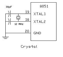
Figure 3.4: Crystal Oscillator Circuit
RESET
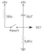
Figure 3.5: RESET Pin Circuit
RESET is an active High input When RESET is set to High, 8052 goes back to the power on state. The 8052 is reset by holding the RST high for at least two machine cycles and then returning it low. Initially charging of capacitor makes RST High, When capacitor charges fully it blocks DC.
SIP Resistor
Sip Resistor is a single in pack Resistor (i.e.,) 8 resistors connected in series. Basically SIP resistor is a 9 pin connector first pin is for power supply to the entire 8 resistors in SIP.
Generally SIP Resistor is used to close the open drain connections of Port 0.
3.4. RFID Reader
Figure 3.6: RFID Reader
Radio Frequency Identification (RFID) Card Readers give an ease answer for read latent RFID transponder labels up to 7 cm away. This RFID Card Reader can be utilized as a part of a wide assortment of specialist and business applications, including access control, programmed ID, apply autonomy route, stock following, installment frameworks, and auto immobilization. The RFID card peruser read the RFID tag in range and yields exceptional distinguishing proof code of the tag at baud rate of 9600. The information from RFID peruser can be interfaced to be perused by microcontroller or PC.
Radio-recurrence ID (RFID) is a programmed ID strategy, depending on putting away and remotely recovering information utilizing gadgets called RFID labels or transponders. The innovation requires some degree of collaboration of a RFID peruser and a RFID tag. A RFID tag is a protest that can be connected to or joined into an item, creature, or individual with the end goal of recognizable proof and following utilizing radio waves. A few labels can be perused from a few meters away and past the viewable pathway of the peruser.
What is RFID?
An essential RFID framework comprises of three segments:
a) A radio wire or curl
b) A handset (with decoder)
c) A transponder (RF tag)
Electronically modified with extraordinary information.There are a wide range of sorts of RFID frameworks out in the market. They are sorted by their recurrence ranges. Probably the most ordinarily utilized RFID units are as per the following:
1. Low-recurrence (30 KHz to 500 KHz)
2. Mid-Frequency (900KHz to 1500MHz)
3. High Frequency (2.4GHz to 2.5GHz)
These recurrence extends for the most part tell the RF scopes of the labels from low recurrence tag going from 3m to 5m, mid recurrence running from 5m to 17m and high recurrence going from 5ft to 90ft. The cost of the framework is based by their reaches with low-recurrence framework going from a couple of hundred dollars to a high-recurrence framework extending some place close to 5000 dollars.
Radio Frequency Identification (RFID) Card Readers give a minimal effort answer for read detached RFID transponder labels up to 2 inches away. The RFID Card Readers can be utilized as a part of a wide assortment of specialist and business applications, including access control, programmed recognizable proof, mechanical technology route, stock following, installment frameworks, and auto immobilization. The RFID card peruser read the RFID tag in range and yields remarkable distinguishing proof code of the tag at baud rate of 9600. The information from RFID peruser can be interfaced to be perused by microcontroller or PC.
Highlights
1. Low-cost strategy for perusing aloof RFID transponder labels
2. 9600 bps serial interface at RS232 level
3. Buzzer and LED demonstrate substantial RFID Tag discovery
4. RS232 interface associates straightforwardly to PC, Mac or Linux machine and requires no extra wiring.
RFID Reader Package Includes
- RFID Reader (Assembled and Tested with 1 year guarantee)
- Serial Cable
- Data
Every transponder tag contains a one of a kind identifier (one of 240, or 1,099,511,627,776 conceivable blends) that is perused by the RFID Card Reader and transmitted to the host by means of a basic serial interface. It implies no two labels are same. Each tag has diverse esteem. This esteem if read by peruser.
Correspondence
At the point when the RFID Card Reader is dynamic and a legitimate RFID transponder tag is put inside scope of the actuated peruser, the one of a kind ID will be transmitted as a 12-byte printable ASCII string serially to the host in the accompanying arrangement:
The begin byte and stop byte are utilized to effectively recognize that a right string has been gotten from the peruser (they relate to a line bolster and carriage return characters, individually). The center ten bytes are the real label’s one of a kind ID. For instance, for a tag with a legitimate ID of 0F0184F07A, the accompanying ASCII information would be sent 0F0184F07A Same information in HEX bytes can be deciphered as: 0x0A, 0x30, 0x46, 0x30, 0x31, 0x38, 0x34, 0x46, 0x30, 0x37, 0x41, 0x0D All correspondence is 8 information bits, no equality, 1 stop bit, and minimum huge piece initial (8N1). The baud rate is arranged for 9600 bps, a standard interchanges speed bolstered by most any chip or PC, and can’t be changed. The RFID Card Reader starts all correspondence. This permits simple access to the serial information stream from any programming dialect that can open a COM port.
Utilizing RFID Reader
At the point when controlled on the RFID peruser will actuate a RF field sitting tight for a tag to come into its range. When tag is recognized, its one of a kind ID number is perused and information is sent by means of serial interface. The substantial label distinguishing is demonstrated by LED flicker and Buzzer beep. The substance of the RFID tag ought to be held parallel to the front of the radio wire (where the greater part of RF vitality is engaged). In the event that the tag is held sideways (opposite to the radio wire) you may experience issues persuading the tag to be perused. Just a single transponder tag ought to be held up to the reception apparatus whenever. The utilization of numerous labels at one time will bring about label impacts and befuddle the peruser. The labels accessible with us have a perused separation of around 2 inches. Genuine separation may fluctuate marginally relying upon the span of the transponder tag and ecological states of the application. On PC you can utilize programming like hyper terminal which can demonstrate ASCII information at 9600 baud rate. You can likewise create programming in any dialect which can interface with serial port and tune in for approaching ASCII information.
Power Requirement of Receiver
The unit needs around 200mA power to operate at 12V. You can use any readymade 12V 500mA DC Adapter or design a transformer plus rectifier based 12V DC power for the board. You can also use just the 12V transformer as the board has bridge and capacitor to convert to DC. We recommend SMPS based 12V 1A DC Adapter for 24 hours operation as it is efficient and does not generate heat as compared to transformer based adapters. Serial Cable connections for RS232 interfacing (Provided with product) To use with a PC serial port, use a serial cable of male-female type with pins 2,3,5 connected to 2,3,5 straight(no cross over cable).
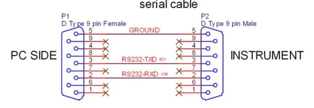
Figure 3.7: RFID Power requirement
Connecting to PC
Use the supplied serial cable to connect to PC’s serial port. Use Hyperterminal software which comes with Windows XP or use any other Terminal software with following settings.
Data Rate: 9600 Data Bits: 8 Parity: None Stop Bit: 1 Flow Control: None
RFID Technology Overview
Radio Frequency Identification (RFID) is a non specific term for non-reaching advances that utilization radio waves to consequently distinguish individuals or articles. There are a few techniques for distinguishing proof, yet the most well-known is to store an interesting serial number that recognizes a man or protest on a microchip that is joined to a reception apparatus. The joined reception apparatus and microchip are called a “RFID transponder” or “RFID tag” and work in mix with a “RFID peruser” (once in a while called a “RFID investigator”). A RFID framework comprises of a peruser and at least one labels. The peruser’s reception apparatus is utilized to transmit radio recurrence (RF) vitality. Contingent upon the label sort, the vitality is “gathered” by the label’s reception apparatus and used to control up the inner hardware of the tag. The tag will then tweak the electromagnetic waves produced by the peruser with a specific end goal to transmit its information back to the peruser. The peruser gets the adjusted waves and changes over them into advanced information. There are two noteworthy sorts of label advancements. “Inactive labels” are labels that don’t contain their own energy source or transmitter. At the point when radio waves from the peruser achieve the chip’s recieving wire, the vitality is changed over by the reception apparatus into power that can control up the microchip in the tag (known as “parasitic power”). The tag is then ready to send back any data put away on the tag by mirroring the electromagnetic waves as depicted previously. “Dynamic labels” have their own particular power source and transmitter.
The power source, normally a battery, is utilized to run the microchip’s hardware and to communicate a flag to a peruser. Because of the way that aloof labels don’t have their own transmitter and must mirror their flag to the peruser, the perusing separation is considerably shorter than with dynamic labels. In any case, dynamic labels are regularly bigger, more costly, and require intermittent administration. The RFID Card Reader is composed particularly for uninvolved labels. Recurrence alludes to the extent of the radio waves used to impart between the RFID framework parts. Similarly as you tune your radio to various frequencies with a specific end goal to hear diverse radio stations, RFID labels and perusers must be tuned to a similar recurrence keeping in mind the end goal to impart adequately. There truly is no such thing as an “average” RFID tag. The read scope of a tag eventually relies on upon many components: the recurrence of RFID framework operation, the energy of the peruser, natural conditions, physical size of the labels reception apparatus and obstruction from other RF gadget. Adjusting various building exchange offs (reception apparatus estimate v. perusing separation v. control v. fabricating cost), the Sunrom RFID Card Reader’s radio wire was planned with a RFID operation at a label read separation of around 4 inches.
Parts Of RFID
An essential RFID framework comprise of three segments:
1) An radio wire or curl
2) A handset (with decoder)
3) A transponder (RF tag) electronically modified with exceptional data
1. Recieving wire
The recieving wire discharges radio signs to enact the tag and read and compose information to it. Reception apparatuses are the channels between the tag and the handset, which controls the framework’s information securing and correspondence. Radio wires are accessible in an assortment of shapes and sizes; they can be incorporated with a door jamb to get label information from people or things going through the entryway, or mounted on an interstate tollbooth to screen activity going by on a turnpike. The electromagnetic field delivered by a recieving wire can be always present when numerous labels are normal consistently. On the off chance that steady cross examination is not required, a sensor gadget can initiate the field. Frequently the radio wire is bundled with the handset and decoder to end up plainly a peruser (a.k.a. investigative specialist), which can be designed either as a handheld or a settled mount gadget.
The peruser emanates radio waves in scopes of somewhere in the range of one inch to 100 feet or all the more, contingent on its energy yield and the radio recurrence utilized. At the point when a RFID label goes through the electromagnetic zone, it identifies the peruser’s actuation flag. The peruser deciphers the information encoded in the label’s coordinated circuit (silicon chip) and the information is passed to the host PC for preparing.
2. TAG
A RFID tag is included a microchip containing recognizing data and a radio wire that transmits this information remotely to a peruser. At its most fundamental, the chip will contain a serialized identifier, or tag number, that exceptionally distinguishes that thing, like the way many standardized tags are utilized today. A key contrast, however is that RFID labels have a higher information limit than their standardized identification partners. This builds the choices for the sort of data that can be encoded on the tag, including the maker, clump or part number, weight, possession, goal and history, (for example, the temperature range to which a thing has been uncovered). Truth be told, a boundless rundown of different sorts of data can be put away on RFID labels, contingent upon application needs. A RFID tag can be set on individual things, cases or beds for distinguishing proof purposes, and on settled resources, for example, trailers, compartments, totes, and so forth Tags arrive in an assortment of sorts, with an assortment of capacities. Key factors include: “Read-just” versus “read-state” There are three alternatives as far as how information can be encoded on labels: (1) Read-just labels contain information, for example, a serialized following number, which is pre-composed onto them by the label maker or merchant. These are for the most part the slightest costly labels since they can’t have any extra data included as they move all through the production network. Any updates to that data would need to be kept up in the application programming that tracks SKU development and action. (2) “Compose once” labels empower a client to compose information to the label one time underway or appropriation forms. Once more, this may incorporate a serial number, yet maybe other information, for example, a great deal or group number. (3) Full “read-express” labels permit new information to be composed to the tag as required and even composed over the first information. Cases for the last capacity may incorporate the time and date of possession exchange or refreshing the repair history of a settled resource. While these are the most expensive of the three label sorts and are not reasonable for following economical things, future gauges for electronic item codes (EPC) have all the earmarks of being traveled toward this path.
Information Capacity
The measure of information stockpiling on a tag can differ, going from 16 bits on the low end to as much as a few thousand bits on the top of the line. Obviously, the more prominent the capacity limit, the higher the cost per tag.
Frame Factor
The tag and recieving wire structure can arrive in an assortment of physical shape calculates and can either act naturally contained or inserted as a component of a customary mark structure (i.e., the tag is inside what resembles a consistent scanner tag name this is named a ‘Shrewd Label’) organizations must pick the fitting structure variables for the tag deliberately and ought to hope to utilize numerous frame elements to suit the labeling needs of various physical items and units of measure. For instance, a bed may have a RFID tag fitted just to a range of ensured arrangement on the bed itself. Then again, containers on the bed have RFID labels inside standardized identification marks that likewise give administrators comprehensible data and a move down ought to the label fall flat or go through non RFID-fit store network joins.
Frequencies
Like every single remote correspondence, there are an assortment of frequencies or spectra through which RFID labels can speak with perusers. Once more, there are exchange offs among cost, execution and application necessities. For example, low-recurrence labels are less expensive than ultra high recurrence (UHF) labels, utilize less power and are better ready to enter non-metallic substances. They are perfect for checking objects with high water substance, for example, natural product, at short proximity. UHF frequencies commonly offer better range and can exchange information speedier. Be that as it may, they utilize more power and are less inclined to go through a few materials. UHF labels are normally most appropriate for use with or close wood, paper, cardboard or attire items. Contrasted with low recurrence labels, UHF labels may be better to scan boxes of products as they go through an inlet entryway into a stockroom. While the label necessities for consistence commands might be barely characterized, it is likely that an assortment of label sorts will be required to illuminate particular operational issues. You will need to work with an organization that is exceptionally learned in tag and peruser innovation to suitably distinguish the correct blend of RFID innovation for your condition and applications.
EPC Tags
EPC suggests “electronic thing code,” a rising assurance for RFID marks, per clients and business applications at first made at the Auto-ID Center at the Massachusetts Institute of Technology. This affiliation has given critical insightful activity toward the use and utilization of RFID advancement. EPC addresses a specific approach to manage thing recognizing confirmation, including a rising standard for the marks themselves, including both the data substance of the tag and open remote correspondence traditions. One might say, the EPC improvement is merging the data standards typified in certain institutionalized label conclusions, for instance, the UPC or UCC-128 scanner label benchmarks, with the remote data correspondence gages that have been created by ANSI and diverse get-togethers.
3. RF Transceiver
The RF handset is the wellspring of the RF vitality used to initiate and power the inactive RFID labels. The RF handset might be encased in an indistinguishable bureau from the peruser or it might be a different bit of gear. At the point when given as a different bit of hardware, the handset is regularly alluded to as a RF module. The RF handset controls and tweaks the radio frequencies that the reception apparatus transmits and gets. The handset channels and opens up the backscatter motion from a uninvolved RFID
3.5 .MAX 232 IC
Max232 IC is a specialized circuit which makes standard voltages as required by RS232 standards. This IC provides best noise rejection and very reliable against discharges and short circuits. MAX232 IC chips are commonly referred to as line drivers.
Figure 3.9: MAX232 IC
To guarantee information exchange amongst PC and microcontroller, the baud rate and voltage levels of Microcontroller and PC ought to be the same. The voltage levels of microcontroller are logic1 and rationale 0 i.e., rationale 1 is +5V and rationale 0 is 0V. In any case, for PC, RS232 voltage levels are considered and they are: rationale 1 is taken as – 3V to – 25V and rationale 0 as +3V to +25V. Along these lines, to break even with these voltage levels, MAX232 IC is utilized. Subsequently this IC changes over RS232 voltage levels to microcontroller voltage levels and the other way around.
Pin Configuration and Functions
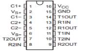 Figure 3.10: MAX 232 Pin diagramss
Pin Description
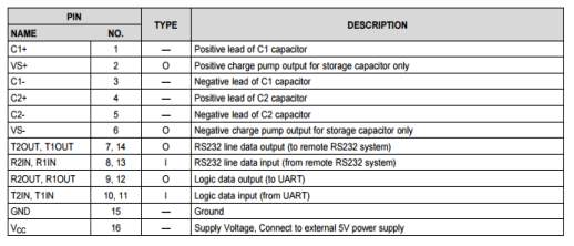
Table 3.1:MAX232 Pin description
The MAX232 IC is used to change over the TTL/CMOS method of reasoning levels to RS232 justification levels in the midst of serial correspondence of microcontrollers with PC. The controller works at TTL method of reasoning level (0-5V) while the serial correspondence in PC wears down RS232 measures (- 25 V to + 25V). This makes it difficult to develop a prompt association between them to talk with each other.
The midway association is given through MAX232. It is a twofold driver/recipient that fuses a capacitive voltage generator to supply RS232 voltage levels from a lone 5V supply. Each recipient adherents RS232 commitments to 5V TTL/CMOS levels. These beneficiaries (R1 and R2) can recognize ±30V inputs. The drivers (T1 and T2), also called transmitters, change over the TTL/CMOS input level into RS232 level.
The transmitters take commitment from controller’s serial transmission stick and send the respect RS232’s beneficiary. The beneficiaries, on the other hand, take commitment from transmission stick of RS232 serial port and give serial respect microcontroller’s authority stick. MAX232 needs four outside capacitors whose regard ranges from 1µF to 22µF.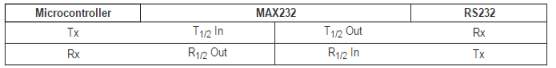
Features
Operates From a Single 5-V Power Supply With 1.0-µF Charge-Pump Capacitors
Operates up to 120 kbit/s
Two Drivers and Two Receivers
±30-V Input Levels
Low Supply Current: 8 mA Typical
Applications
- TIA/EIA-232-F
- Battery-Powered Systems
- Terminals
- Modems
- Computers
3.6. Liquid Crystal Display
LCD remains for Liquid Crystal Display. LCD is finding boundless utilize supplanting LEDs (seven section LEDs or other multi portion LEDs) due to the accompanying reasons:
1.The declining costs of LCDs.
2.The capacity to show numbers, characters and design. This is as opposed to LEDs, which are constrained to numbers and a couple characters.
3.Incorporation of an invigorating controller into the LCD, consequently assuaging the CPU of the assignment of reviving the LCD. Conversely, the LED must be invigorated by the CPU to continue showing the information.
4.Ease of programming for characters and design.
These segments are “specific” for being utilized with the microcontrollers, which implies that they can’t be initiated by standard IC circuits. They are utilized for composing diverse messages on a small scale LCD.
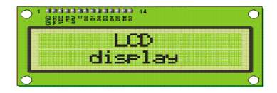
Figure 3.11:LCD display
A model portrayed here is at its ease and awesome potential outcomes most as often as possible utilized as a part of practice. It depends on the HD44780 microcontroller (Hitachi) and can show messages in two lines with 16 characters each. It shows every one of the letter sets, Greek letters, accentuation marks, scientific images and so on. Moreover, it is conceivable to show images that client makes up all alone.
Programmed moving message in plain view (move left and right), appearance of the pointer, backdrop illumination and so forth are considered as valuable attributes.
A. Pins Functions
There are sticks along one side of the little printed board utilized for association with the microcontroller. There are aggregate of 14 pins set apart with numbers (16 on the off chance that the foundation light is implicit). Their capacity is depicted in the table 3.6:
Table 3.2: Pin functions of LCD
| Pin No | Function | Name |
| 1 | Ground (0V) | Ground |
| 2 | Supply Voltage, 5V(4.7 V-5.3V) | Vcc |
| 3 | Contrast adjustment, through a variable resistor | VEE |
| 4 | Selects command register when low, and the register when high | Register select |
| 5 | Low to write to the register, high to read from the register | Read /Write |
| 6 | Sends data to data pins when a high to low pulse is given | Enable |
| 7 | DB0 | |
| 8 | DB1 | |
| 9 | DB2 | |
| 10 | 8- BIT DATA PINS | DB3 |
| 11 | DB4 | |
| 12 | DB5 | |
| 13 | DB6 | |
| 14 | DB7 | |
| 15 | Backlight Vcc(5V) | Led + |
| 16 | Backlight ground(0V) | Led+ |
B. LCD screen
LCD screen appeared in figure 3.15 comprises of two lines with 16 characters each. Each character comprises of 5×7 dab framework. Differentiate in plain view relies on upon the power supply voltage and whether messages are shown in maybe a couple lines. Hence, factor voltage 0-Vdd is connected on stick set apart as Vee. Trimmer potentiometer is generally utilized for that reason. A few variants of presentations have worked in backdrop illumination (blue or green diodes). At the point when utilized amid working, a resistor for current confinement ought to be utilized (like with any LE diode).
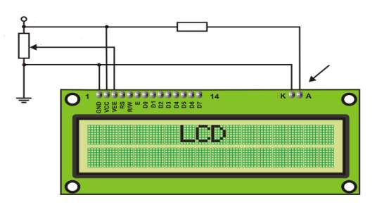 Figure3.12: LCD connection
Contrast
LCD backlight
330R
5k
C. LCD Basic Commands
All data traded to LCD through yields D0-D7 will be deciphered as requests or as data, which depends on upon justification state on stick RS: RS = 1 – Bits D0 – D7 are areas of characters that should be appeared. Worked in processor addresses worked in “guide of characters” and shows relating pictures. Demonstrating position is controlled by DDRAM address. This address is either in advance portrayed or the address of effectively traded character is actually expanded.
RS = 0 – Bits D0 – D7 are charges which choose indicate mode. Once-over of summons which LCD sees are basic to form the code for LCD. The underneath table 3.4 exhibits the LCD summons which are significant in the composed work of code to demonstrate the data.
Table 3.3: LCD commands table
| Command | RS | RW | D7 | D6 | D5 | D4 | D3 | D2 | D1 | D0 | Execution
Time |
|
| Clear display | 0 | 0 | 0 | 0 | 0 | 0 | 0 | 0 | 0 | 1 | 1.64Ms | |
| Cursor home | 0 | 0 | 0 | 0 | 0 | 0 | 0 | 0 | 1 | x | 1.64mS | |
| Entry mode set | 0 | 0 | 0 | 0 | 0 | 0 | 0 | 1 | I/D | S | 40uS | |
| Display on/off control | 0 | 0 | 0 | 0 | 0 | 0 | 1 | D | U | B | 40uS | |
| Cursor/Display Shift | 0 | 0 | 0 | 0 | 0 | 1 | D/C | R/L | x | x | 40uS | |
| Function set | 0 | 0 | 0 | 0 | 1 | DL | N | F | x | x | 40uS | |
| Set CGRAM address | 0 | 0 | 0 | 1 | CGRAM address | 40uS | ||||||
| Set DDRAM address | 0 | 0 | 1 | DDRAM address | 40uS | |||||||
| Read “BUSY” flag (BF) | 0 | 1 | BF | DDRAM address | – | |||||||
| Write to CGRAM or DDRAM | 1 | 0 | D7 | D6 | D5 | D4 | D3 | D2 | D1 | D0 | 40uS | |
| Read from CGRAM or DDRAM | 1 | 1 | D7 | D6 | D5 | D4 | D3 | D2 | D1 | D0 | 40uS | |
I/D 1 = Increment (by 1) R/L 1 = Shift right
0 = Decrement (by 1) 0 = Shift left
S 1 = Display shift on DL 1 = 8-bit interface
0 = Display shift off 0 = 4-bit interface
D 1 = Display on N 1 = Display in two lines
0 = Display off 0 = Display in one line
U 1 = Cursor on F 1 = Character format 5×10 dots
0 = Cursor off 0 = Character format 5×7 dots
B 1 = Cursor blink on D/C 1 = Display shift
0 = Cursor blink off 0 = Cursor shift
D. LCD Connection
Contingent upon what number of lines are utilized for association with the microcontroller, there are 8-bit and 4-bit LCD modes. The fitting mode is resolved toward the start of the procedure in a stage called “instatement”. In the principal case, the information are exchanged through yields D0-D7 as it has been as of now clarified. In the event of 4-bit LED mode, for sparing significant I/O pins of the microcontroller, there are just 4 higher bits (D4-D7) utilized for correspondence, while other might be left detached.
Subsequently, every information is sent to LCD in two stages: four higher bits are sent first (that regularly would be sent through lines D4-D7), four lower bits are sent a while later. With the assistance of instatement, LCD will accurately interface and translate every information got. In addition, with respect to the way that information are once in a while perused from LCD (information for the most part are exchanged from microcontroller to LCD) one more I/O stick might be spared by straightforward associating R/W stick to the Ground. Such sparing has its cost. Despite the fact that message showing will be regularly performed, it won’t be conceivable to peruse from occupied banner since it is unrealistic to peruse from show.
E. LCD Initialization
Once the power supply is turned on, LCD is consequently cleared. This procedure goes on for around 15mS. From that point forward, show is prepared to work. The method of working is set as a matter of course. This implies:
1. Show is cleared
2. Mode
DL = 1 Communication through 8-bit interface
N = 0 Messages are shown in one line
F = 0 Character text style 5 x 8 specks
3. Show/Cursor on/off
D = 0 Display off
U = 0 Cursor off
B = 0 Cursor squint off
3. Character passage
ID = 1 Addresses in plain view are consequently augmented by 1
S = 0 Display move off
Modified reset is mostly performed without any issues. In case for any reason control supply voltage does not accomplish full a motivation over the traverse of 10mS, show will start perform absolutely unconventionally.
In case voltage supply unit can’t meet this condition or if it is relied upon to give absolutely safe working, the strategy of instatement by which another reset enabling introduction to work routinely ought to be associated.
Count as showed by the presentation is being performed depends on upon whether relationship with the microcontroller is through 4-or 8-bit interface. All left over to be done after that is to give principal charges and clearly to show messages.
F. Contrast control
To have a clear view of the characters on the LCD, contrast should be adjusted. To adjust the contrast, the voltage should be varied. For this, a preset is used which can behave like a variable voltage device. As the voltage of this preset is varied, the contrast of the LCD can be adjusted.


Wiper
Track
Terminals
Figure 3.13: Variable resistor
G. Potentiometer
Variable resistors appeared in figure 3.16 utilized as potentiometers have each of the three terminals associated. This plan is ordinarily used to fluctuate voltage, for instance to set the exchanging purpose of a circuit with a sensor, or control the volume (commotion) in an intensifier circuit. On the off chance that the terminals at the finishes of the track are associated over the power supply, then the wiper terminal will give a voltage which can be fluctuated from zero up to the most extreme of the supply. The image of potentiometer is appeared in figure 3.17.
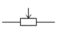
Figure 3.14: Potentiometer symbol
H. Presets
These are smaller than normal adaptations of the standard variable resistor. They are intended to be mounted specifically onto the circuit board and balanced just when the circuit is assembled. For instance, to set the recurrence of an alert tone or the affectability of a light-delicate circuit, a little screwdriver or comparative instrument is required to alter presets.
Presets are considerably less expensive than standard variable resistors so they are some of the time utilized as a part of activities where a standard variable resistor would regularly be utilized. Preset image is appeared in figure 3.18. Multiturn presets are utilized where extremely exact changes must be made. The screw must be turned ordinarily (10+) to move the slider from one end of the track to the next, giving fine control.

Figure 3.15: Preset symbol
3.7. GSM Module
The short message framework (SMS) of a standard cell phone can be utilized for a great deal something other than trading secretive message. This application finds an unassuming portable working for controlling outside types of gear. The SMS benefit gives by the specialist co-ops are relatively minimal effort. Subsequently the framework is profoundly proficient and ease.
Cell phones have turned into an across the board methods for correspondence. It turns into a piece of regular day to day existence with perpetually individuals getting a charge out of the administration and additional opportunity they give. It deals with the premise of Global System for Mobile Communication (GSM). An endorser from any frameworks can get to media transmission benefits by utilizing a Subscriber Identify Module (SIM) card in a handset appropriate for the system on the went by framework The Short Message Service permits instant messages to be sent and got to and from cell phones. The content can contain words or numbers or an alphanumeric blend. Since Simple individual – to – individual informing is such a vital part of aggregate SMS movement volumes, anything that streamlines message era and in addition amplified utility of the SMS being sent is an essential empowering agent of Short Message Service.
Figure 3.16: GSM Module
The primary point of this venture is to control the auto motor. We will interface Hardware unit to auto motor. The equipment unit comprises of microcontroller and GSM modem
A GSM modem is a specific kind of modem which acknowledges a SIM card, and works over a membership to a portable administrator, much the same as a cell phone. From the portable administrator point of view, a GSM modem looks simply like a cell phone.
At the point when a GSM modem is associated with a PC, this permits the PC to utilize the GSM modem to convey over the versatile system. While these GSM modems are most much of the time used to give versatile web network, a number of them can likewise be utilized for sending and getting SMS and MMS messages.
Presently SMS Light can send and get SMS and MMS Messages utilizing a GSM modem:
A GSM modem can be a devoted modem gadget with a serial, USB or Bluetooth association, or it can be a cell phone that gives GSM modem abilities.
With the end goal of this record, the term GSM modem is utilized as a bland term to allude to any modem that backings at least one of the conventions in the GSM developmental family, including the 2.5G innovations GPRS and EDGE, and additionally the 3G advances WCDMA, UMTS, HSDPA and HSUPA.
A GSM modem uncovered an interface that permits applications, for example, Now SMS to send and get messages over the modem interface. The versatile administrator charges for this message sending and getting as though it was performed specifically on a cell phone. To play out these undertakings, a GSM modem must support a “stretched out AT summon set” for sending/getting SMS messages, as characterized in the ETSI GSM 07.05 and 3GPP TS 27.005 details.
GSM modems can be a fast and proficient approach to begin with SMS, on the grounds that an extraordinary membership to a SMS specialist organization is not required. In many parts of the world, GSM modems are a practical answer for accepting SMS messages, in light of the fact that the sender is paying for the message conveyance.
A GSM modem can be a devoted modem gadget with a serial, USB or Bluetooth association, for example, the Falcon Samba 75. (Different producers of committed GSM modem gadgets incorporate Wavecom, Multitech and iTegno. We’ve likewise evaluated various modems on our specialized bolster blog.) To start, embed a GSM SIM card into the modem and associate it to an accessible USB port on your PC.
A GSM modem could likewise be a standard GSM cell phone with the proper link and programming driver to interface with a serial port or USB port on your PC. Any telephone that backings the “reached out AT charge set” for sending/getting SMS messages, as characterized in ETSI GSM 07.05 as well as 3GPP TS 27.005, can be upheld by the Now SMS and MMS Gateway. Take note of that not every cell phone bolster this modem interface.
Because of some similarity issues that can exist with cell phones, utilizing a devoted GSM modem is normally desirable over a GSM cell phone. This is a greater amount of an issue with MMS informing, where in the event that you wish to have the capacity to get inbound MMS messages with the portal, the modem interface on most GSM telephones will just permit you to send MMS messages. This is on the grounds that the cell phone consequently forms got MMS message warnings without sending them by means of the modem interface. It ought to likewise be noticed that not all telephones bolster the modem interface for sending and getting SMS messages. Specifically, most advanced mobile phones, including Blackberries, iPhone, and Windows Mobile gadgets, don’t bolster this GSM modem interface for sending and accepting SMS messages at all by any stretch of the imagination. Also, Nokia telephones that utilization the S60 (Series 60) interface, which is Symbian based, just bolster sending SMS messages by means of the modem interface, and don’t bolster getting SMS by means of the modem interface.
The Future of GSM
GSM together with different advancements is a piece of a development of remote versatile media transmission that incorporates High-Speed Circuit-Switched Data (HSCSD), General Packet Radio System (GPRS), Enhanced Data rate for GSM Evolution (EDGE), and Universal Mobile Telecommunications Service (UMTS).
GSM Network Operators
T-Mobile and Cingular work GSM arranges in the United States on the 1,900 MHz band. GSM organizes in different nations work at 900, 1,800, or 1,900 MHz.
GSM (Global System for Mobile Communications)
Initially from Group Special Mobile) is the most well known standard for versatile communication frameworks on the planet. The GSM Association, its advancing industry exchange association of cell phone bearers and makers, evaluates that 80% of the worldwide versatile market utilizes the standard.[1] GSM is utilized by more than 1.5 billion people[2] crosswise over more than 212 nations and territories.[3] This pervasiveness implies that supporters can utilize their telephones all through the world, empowered by universal meandering courses of action between portable system administrators. GSM varies from its ancestor innovations in that both flagging and discourse channels are advanced, and in this way GSM is viewed as a moment era (2G) cell phone framework. This likewise encourages the across the board execution of information correspondence applications into the framework.
The GSM standard has been favorable position to both buyers, who may profit by the capacity to meander and switch transporters without supplanting telephones, and furthermore to network administrators, who can pick gear from numerous GSM hardware vendors.[4] GSM likewise spearheaded minimal effort usage of the short message benefit (SMS), additionally called content informing, which has since been bolstered on other cell phone norms too. The standard incorporates an overall crisis phone number component (112).[5]
More current renditions of the standard were in reverse good with the first GSM framework. For instance, Release ’97 of the standard included parcel information capacities by methods for General Packet Radio Service (GPRS). Discharge ’99 presented higher speed information transmission utilizing Enhanced Data Rates for GSM Evolution (EDGE).
GSM transporter frequencies
GSM systems work in various distinctive transporter recurrence ranges (isolated into GSM recurrence ranges for 2G and UMTS recurrence groups for 3G), with most 2G GSM systems working in the 900 MHz or 1800 MHz groups. Where these groups were at that point apportioned, the 850 MHz and 1900 MHz groups were utilized rather (for instance in Canada and the United States). In uncommon cases the 400 and 450 MHz recurrence groups are doled out in a few nations since they were already utilized for original frameworks.
Most 3G systems in Europe work in the 2100 MHz recurrence band.
Notwithstanding the recurrence chose by an administrator, it is partitioned into timeslots for individual telephones to utilize. This permits eight full-rate or sixteen half-rate discourse channels per radio recurrence. These eight radio timeslots (or eight burst periods) are gathered into a TDMA outline. Half rate directs utilize exchange outlines in the same timeslot. The channel information rate for every one of the 8 channels is 270.833 Kbit/s, and the edge span is 4.615 ms.
The transmission control in the handset is constrained to a most extreme of 2 watts in GSM850/900 and 1 watt in GSM1800/1900.
Check if your GSM telephone or modem bolsters SMS content mode:
To check if your modem underpins this content mode, you can attempt the accompanying charge:
AT+CMGF=1 <ENTER>
On the off chance that the modem reacts with “alright” this mode is upheld. Kindly note that utilizing this mode it is just conceivable to send basic instant messages. It is unrealistic to send multipart, Unicode, information and different sorts of messages.
Setting up the modem
In the event that the modem contains a SIM card with is secured with a PIN code, we need to enter this stick code first:
AT+CPIN=”0000″ <ENTER> (supplant 0000 with your PIN code):
If you don’t mind not that much of the time you have just 3 endeavors to set the right PIN code. Subsequent to setting the PIN code, hold up a few seconds before issuing the following charge to give the modem some an opportunity to enlist with the GSM organize.
So as to send a SMS, the modem must be placed in SMS content mode first utilizing the accompanying summon:
AT+CMGF=1 <ENTER>
In content mode there are some extra parameters that can be set. Utilizing the accompanying order we can read the present qualities:
AT+CSMP? <ENTER>
The modem wills reaction with a string this way:
+CSMP: 1, 169, 0,0OK
The main esteem is a blend of some alternative bits:
bit 7 RP Reply way, not utilized as a part of content mode
bit 6 UDHI User Data Header Information
bit 5 SRR Set this bit to ask for a conveyance report
bit 3,4 VPF Validity Period, set b4=1 if a VP esteem is available
bit 2 RD Reject Duplicates, don’t give back a message ID when a message with a similar goal and ID is as yet pending
bit 0,1 MTI Message Type Indicatorb1=0 and b0=0 – > SMS-DELIVERb1=0 and b0=1 – > SMS-SUBMIT
Bit 0 of the message is constantly set when sending messages (SMS-SUBMIT). So the main esteem ought to be 1 or higher. The second parameter sets the Validity Period of the message. This esteem is encoded as takes after:
0 – 143 (VP + 1) x 5 minutes
144 – 167 12 Hours + ((VP-143) x 30 minutes)
168 – 196 (VP-166) x 1 day
197 – 255 (VP-192) x 1 week
The third parameter contains the PID (Protocol Identifier). This parameter is utilized for cutting edge informing. The fourth parameter contains the DCS (Data Coding Scheme). This parameter is utilized to choose the character set/message sort. When setting the DCS parameter to “0” standard 7 bit content is send. When setting this parameter to “16” the message is sent as a blaze message.
To communicate something specific with a legitimacy time of 1 day, the parameters must be set this way:
Bit 0 and 4 of the primary field must be set, so the main esteem will progress toward becoming 1 + 16 = 17.
Send the accompanying order to the modem to set this parameters:
AT+CSMP=17, 167,0,16 <ENTER>
On the off chance that the m
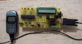
Figure 3.17: GSM module connection to phone
The message will arrive on the mobile phone shortly.
CHAPTER 4
SOFTWARE TOOLS
This chapter briefly explains about the firmware implementation of the project
4.1. Source Code
- Click on the Keil uVision Icon on Desktop
- The following fig will appear
- Click on the Project menu from the title bar
- Then Click on New Project
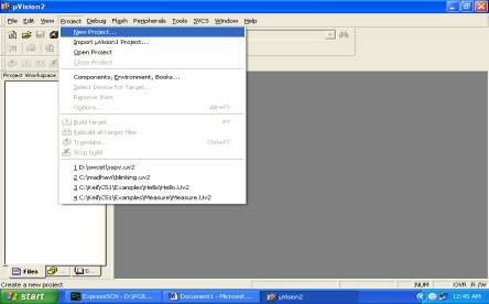
- Save the Project by typing suitable project name with no extension in u r own folder sited in either C: or D:
- Then Click on Save button above.
- Select the component for u r project. i.e. Atmel……
- Click on the + Symbol beside of Atmel
- Select AT89C51 as shown below
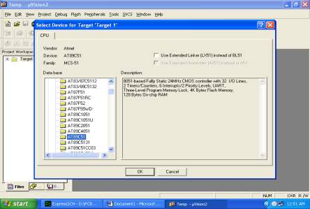
- Then Click on “OK”
- The Following fig will appear
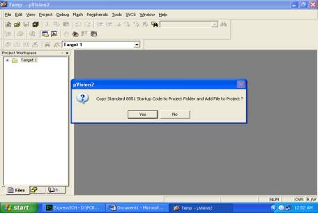
- Then Click either YES or NO………mostly “NO”
- Now your project is ready to USE
- Now double click on the Target1, you would get another option “Source group 1” as shown in next page.
- Click on the file option from menu bar and select “new”
- The next screen will be as shown in next page, and just maximize it by double clicking on its blue boarder.
- Now start writing program in either in “C” or “ASM”
- For a program written in Assembly, then save it with extension “. asm” and for “C” based program save it with extension “ .C”
- Now right click on Source group 1 and click on “Add files to Group Source”
- Now you will get another window, on which by default “C” files will appear.
- Now select as per your file extension given while saving the file
- Click only one time on option “ADD”
- Now Press function key F7 to compile. Any error will appear if so happen.
- If the file contains no error, then press Control+F5 simultaneously.
- The new window is as follows
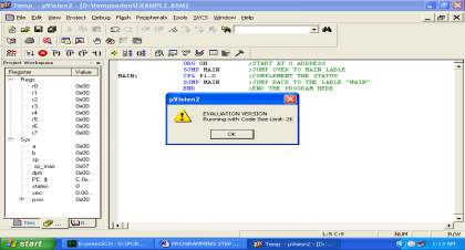
- Then Click “OK”
- Now Click on the Peripherals from menu bar, and check your required port as shown in fig below
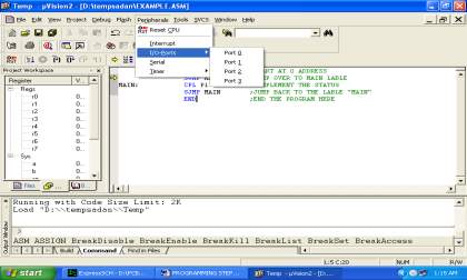
- Drag the port a side and click in the program file.
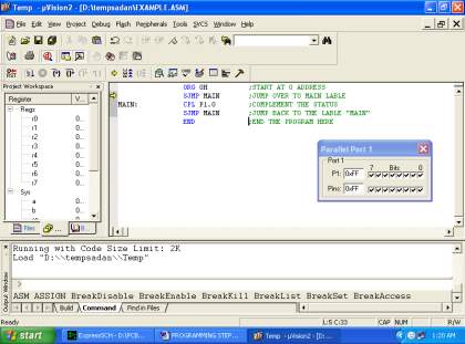
- Now keep Pressing function key “F11” slowly and observe.
- You are running your program successfully
4.2.Proload
Proload is programming which acknowledges just hex records. Once the machine code is changed over into hex code, that hex code must be dumped into the microcontroller and this is finished by the Proload. Proload is a developer which itself contains a microcontroller in it other than the one which is to be customized. This microcontroller has a program in it written such that it acknowledges the hex record from the Keil compiler and dumps this hex document into the microcontroller which is to be modified. As the Proload software engineer pack requires control supply to be worked, this power supply is given from the power supply circuit composed previously. It ought to be noticed that this software engineer pack contains a power supply segment in the board itself however with a specific end goal to switch on that power supply, a source is required. Therefore this is refined from the power supply board with a yield of 12volts.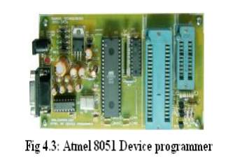
Feature
- Supports major Atmel 89 arrangement gadgets
- Auto Identify associated equipment and gadgets
- Error checking and confirmation in-assembled
- Lock of projects in chip bolstered to forestall program replicating
- 20 and 40 stick ZIF attachment on-board
- Auto Erase before composing and Auto Verify subsequent to composing
- Informative status bar and access to most recent modified record
- Simple and Easy to utilize
- Works on 57600 speed
Portrayal
It is easy to utilize and ease, yet capable blaze microcontroller software engineer for the Atmel 89 arrangement. It will Program, Read and Verify Code Data, Write Lock Bits, Erase and Blank Check. All breaker and bolt bits are programmable. This software engineer has clever locally available firmware and interfaces with the serial port. It can be utilized with a PC and requires no uncommon equipment. All that is required is a serial correspondence ports which all PCs have.
All gadgets have signature bytes that the developer peruses to consequently recognize the chip. No compelling reason to choose the gadget sort, simply connect it to and go! All gadgets additionally have various bolt bits to give different levels of programming and programming security. These bolt bits are completely programmable utilizing this software engineer. Bolt bits are valuable to secure the program to be perused again from microcontroller just permitting delete to reinvent the microcontroller. The developer interfaces with a host PC utilizing a standard RS232 serial port. All the programming “insight” is incorporated with the software engineer so you needn’t bother with any unique equipment to run it. Developer accompanies window based programming for simple programming of the gadgets.
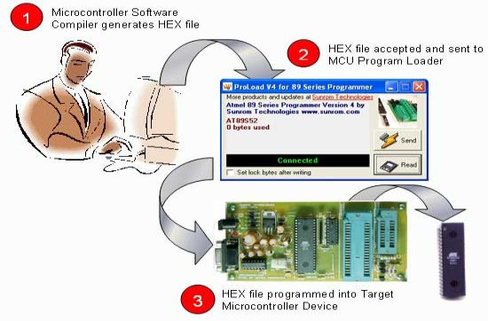
Programming Software
PC side programming called ‘Proload V4.1’ is executed that acknowledges the Intel HEX arrangement document created from compiler to be sent to target microcontroller. It auto identifies the equipment associated with the serial port. It likewise auto recognizes the chip embedded and bytes utilized. Programming is produced in Delphi 7 and requires no overhead of any outside DLL.
CHAPTER 5
SOFTWARE IMPLEMENTATION
5.1 Schematic Diagram
5.2.Flowchart

START

Intialise all devices GSM,LCD & RFID reader


Read RFID card

If
Y=1
 yes
yes
 no
no
Choose the type of grain


Enter the qunatity

If
X=1
 y yes
y yes
Overlimit

no
Take your item(choosen grain name)

Sending message


y=validity of card;x=limit of product
CHAPTER 6
RESULTS AND DISCUSSION
6.1.Implementation Results
The Electronic Distribution Of Goods In Ration Shop depends on GSM and RFID Technology which is utilized for Ration materials dispersion in proportion shops. At first everybody will be given a RFID Card, rather than a proportion card. In the event that the client needs to get any apportion material, the client needs to demonstrate the proportion RFID label card to the RFID per user , the per user will perceive the RFID numbers appear by the client. Every client will have a novel number, which is not noticeable to the client. This perceived RFID number will be given to a microcontroller, which contrasted the info number and the database. Before beginning the framework, the exceptional RFID number of the apportion client will be customized in the controller, for example, User name and secret key, so that the controller will perceive the information originating from RFID by contrasting and the database. Once the client is distinguished, the apportion things to be administered will be shown on the LCD screen, the client needs to bolster the remarks, for example, the weight he will purchase. As the apportioning procedure is going on all the while the controller will send a charge to GSM Modem, to send the content SMS to the client about the proportion thing, he or she obtained

6.2 Advantages
1.Cost viable approach.
2. This framework is exceptionally successful, precise, straightforward and control moderate.
3. Time successful approach.
4. This framework keeps up information accurately.
CHAPTER 7
CONCLUSION AND FUTURE SCOPE
Conclusion
The proportion card is supplanted by brilliant rfid card and client is verified to stay away from phony and great robbery .This proposed venture would make straightforwardness in the framework by making an impression on the client.
Future Scope
In future we can enhance the memory and can store the information of all clients. On the off chance that some goods are not upto the need, data can be sent to both government experts and the card holders utilizing gsm innovation. we can confirm the rfid cards with passwords. we can enhance the consumer loyalty by enhancing the security.
References
[1].Mouly, M., and M. B. Pautet, The Global System for Mobile Communications, 1993.
[2].RFID JOURNAL, 2002-2007, REFFERD 6.8.2007, http://www.rfidjournal.com [8] http://www.vbtutor.net/vb6/vbtutor.html visual basic 6 tutorial.
[3].www.schneiderelectric.com.hk/resources/access/text/rfidreader.
[4].8051 microcontrollers: an applications-based introduction.
[5]. http://elprojects.blogspot.in/2010/03/lcd-pin-description-for-interfacing.html
[6]. Detailed descripton of 8052 http://www.8052.com/tut8052.phtml
Bibliography
[1] Vinayak T. Shelar, Mahadev S. Patil,”RFID and GSM based Automatic Rationing System utilizing LPC2148″, International Journal of Advanced Research in Computer Engineering and Technology (IJARCET) Volume 4 Issue 6, June 2015.
[2] R. Parthipan, K. Sreenivas, “A Systematic Application for Public Distribution-Ration Shop”, International Journal of Innovative Research in Computer and Communication Engineering An ISO 3297: 2007 Certified Organization, Vol.3, Special Issue 6, August 2015.
[3] Abdul H. Ansari, KetanG. Badgujar, Monali R. Rathi, Shital R. Tambe, “Mechanization in proportioning framework utilizing RFID and GSM innovation” International Journal of Engineering, Education and Technology, ISSN 2320-883x, volume 3, issue 2, 01/04/2015.
[4] Kashinath Wakade, Pankaj Chidrawar, Dinesh Aitwade, “Shrewd Ration Distribution and Controlling” International Journal of Scientific and Research Publications, ISSN 2250-3153, Volume 5, Issue 4, April 2015.
[5] Jaid Rahul A, Kadam Chetan K, Kokare Aniket S, Deore Minal, “An Overview of Automatic Rationing System”, International Journal of Informative and Futuristic Research, ISSN 2347-1697, Volume 2 Issue 6 ,February 2015.
[6] Miss. Manisha M. Kadam, Miss. Smita R. Jagdale,Miss Arati A. Lawand, Miss. Shraddha J. Chavan, “Microcontroller Based Efficient Ration Distribution System”, International Journal.
Cite This Work
To export a reference to this article please select a referencing stye below:
Related Services
View all


Related Content
All TagsContent relating to: "Building Materials"
Building materials refers to any material that is used for construction. Many different natural materials were used historically for building such as wood, clay, stone etc. but the material most commonly used in construction is now concrete.
Related Articles

DMCA / Removal Request
If you are the original writer of this dissertation and no longer wish to have your work published on the UKDiss.com website then please: