Operating Home Appliances Remotely Using SMS
Info: 18508 words (74 pages) Dissertation
Published: 3rd Feb 2022
Tagged: Technology
CHAPTER 1: INTRODUCTION
1.1. INTRODUCTION
The aim of this project is to operate the home appliances using SMS from anywhere using mobile and this system also monitors the light status and intimate whenever it fails to glow.
With the present system we need lot of man power to control the switches and most of the time operator forgets to switch off the lights in the morning which results in lot of power wastage. These problems can be solved using present technologies. There are many technologies are coming out to make our lives more comfort, time saving, safer and luxurious. In this project we are using GSM technology.
Cell phones use GSM technology. The microcontroller plays the key role in this project. The GSM modem will be interfaced to the microcontroller which continuously receives the messages from the user cell phone and passes the same to the microcontroller.
The GSM modem will be interfaced to the microcontroller section through serial port interface. If the user wants to operate the lights, he can just send a predefined message to the GSM modem that is interfaced to the controller section. The controller section will have the switch controls of the devices. All the lights which are to be controlled will be connected to the controlling device i.e., to the microcontroller section. The microcontroller in return, sends a message to the mobile number about the status of all the lights.
At controlling side we have GSM modem with one SIM, micro controller, lights controlling circuit, light status detecting feedback system. The user has to send a predefined SMS to the phone number which inserted in modem then modem will indicate this new message to controller ,controller will read this message and control the lights according to message it received. This system also detects light failure condition and sends this information to electricity board.
1.2. OBJECTIVE
The objective of the project is to provide a cost effective solution that will provide controlling of home appliances remotely. The motivation is to facilitate the users to automate their homes having ubiquitous access. The system provides availability due to development of a low cost system. The home appliances control system with an affordable cost was thought to be built that should be mobile providing remote access to the appliances. In addition there was a need to automate home so that user can take advantage of the technological advancement. Therefore this project proposes a system that allows user to be control home appliances ubiquitously via SMS using GSM technology.
1.3. LITERATURE SURVEY
The Public Distribution System (PDS) in the country facilitates the supply of food grains to the poor at a subsidized price. However, doubts have been raised about the efficacy and cost-effectiveness of the PDS, especially in the light of the growing food subsidy and food stocks. The PDS needs to be restructured and there is a need to explore the possibility of introducing innovative ideas such as smart cards, food credit/debit cards, food stamps and decentralized procurement, to eliminate hunger and make food available to the poor wherever they may be in cost-effective manner. To prevent corruption and foster the development of small and medium-sized enterprises, the United Nations Industrial Development Organization (UNIDO) and the United Nations Office on Drugs and Crime (UNODC) have joined forces to carry out this study, which looks at the nature and extent of the problem.
This report is based on field-based assessments and a meeting of experts that discussed obstacles for SME development created by public and private sector corruption. The website will help us to remotely monitor the kerosene outlet and the vehicles providing the kerosene and ration material till it reaches the storage areas and also the distribution at local people will be done centralize through a web application which will keep record of user id and password for every people with solenoid valve, Hooper valve to control openings of ration outlet etc. This will gives assure us no involvement of any person directly with distribution system, also whether kerosene disposition is also sensed at web site using proximity sensor through web giving a clear idea about delivery of it. And also all data is stored at time about ration items and the people who receives the ration from that place.
1.4. EXISTING SYSTEM
In the existing system, the customer uses the ration cards. Ration materials are distributed with the help of humans. This method is inaccurate, tedious and may sometimes results to malpractices
1.5. PROPOSED SYSTEM
In the proposed system, we are using the RFID tags as ration cards. Every product in the supermarket has its unique RFID tag with unique ID. Once the tag is scanned by the RFID reader that product attached to it is read by the RFID reader and sent to the controller. The controller displays the product on the LCD screen and message is sent to both authorities and the card holders with the help of GSM module.
1.6. SCOPE OF STUDY
The scope of study which is needed for the completion of this project involves the following criteria:
Architecture of 8051 knowledge
- 8051 Microcontroller programming in C language.
- Interfacing LCD with Microcontroller.
- Interfacing GSM modem with Microcontroller.
- Connecting the Loads to the Microcontroller.
- The circuitry and devices that is needed to construct the devices and establish the necessary communication between the devices.
- The communication between GSM modem and the 8051 controller will be taken by the serial communication i.e.,MAX232 IC.
- Feedback circuit that identifies the failure detection of the appliances.
CHAPTER 2: INTRODUCTION TO EMBEDDED SYSTEMS
2.1. INTRODUCTION
An embedded system can be defined as a computing device that does a specific focused job. Appliances such as the air-conditioner, VCD player, DVD player, printer, fax machine, mobile phone etc. are examples of embedded systems. Each of these appliances will have a processor and special hardware to meet the specific requirement of the application along with the embedded software that is executed by the processor for meeting that specific requirement. The embedded software is also called “firm ware”. The desktop/laptop computer is a general purpose computer. You can use it for a variety of applications such as playing games, word processing, accounting, software development and so on. In contrast, the software in the embedded systems is always fixed listed below:
Embedded systems do a very specific task, they cannot be programmed to do different things. . Embedded systems have very limited resources, particularly the memory. Generally, they do not have secondary storage devices such as the CDROM or the floppy disk. Embedded systems have to work against some deadlines. A specific job has to be completed within a specific time. In some embedded systems, called real-time systems, the deadlines are stringent. Missing a deadline may cause a catastrophe-loss of life or damage to property. Embedded systems are constrained for power. As many embedded systems operate through a battery, the power consumption has to be very low.
Some embedded systems have to operate in extreme environmental conditions such as very high temperatures and humidity.
2.2. Application Areas
Nearly 99 per cent of the processors manufactured end up in embedded systems. The embedded system market is one of the highest growth areas as these systems are used in very market segment- consumer electronics, office automation, industrial automation, biomedical engineering, wireless communication, data communication, telecommunications, transportation, military and so on.
Consumer appliances
At home we use a number of embedded systems which include digital camera, digital diary, DVD player, electronic toys, microwave oven, remote controls for TV and air-conditioner, VCO player, video game consoles, video recorders etc. Today’s high-tech car has about 20 embedded systems for transmission control, engine spark control, air-conditioning, navigation etc. Even wristwatches are now becoming embedded systems. The palmtops are powerful embedded systems using which we can carry out many general-purpose tasks such as playing games and word processing.
Office automation
The office automation products using em embedded systems are copying machine, fax machine, key telephone, modem, printer, scanner etc.
Industrial automation
Today a lot of industries use embedded systems for process control. These include pharmaceutical, cement, sugar, oil exploration, nuclear energy, electricity generation and transmission. The embedded systems for industrial use are designed to carry out specific tasks such as monitoring the temperature, pressure, humidity, voltage, current etc., and then take appropriate action based on the monitored levels to control other devices or to send information to a centralized monitoring station. In hazardous industrial environment, where human presence has to be avoided, robots are used, which are programmed to do specific jobs. The robots are now becoming very powerful and carry out many interesting and complicated tasks such as hardware assembly.
Medical electronics
Almost every medical equipment in the hospital is an embedded system. These equipments include diagnostic aids such as ECG, EEG, blood pressure measuring devices, X-ray scanners; equipment used in blood analysis, radiation, colonscopy, endoscopy etc. Developments in medical electronics have paved way for more accurate diagnosis of diseases.
Computer networking
Computer networking products such as bridges, routers, Integrated Services Digital Networks (ISDN), Asynchronous Transfer Mode (ATM), X.25 and frame relay switches are embedded systems which implement the necessary data communication protocols. For example, a router interconnects two networks. The two networks may be running different protocol stacks. The router’s function is to obtain the data packets from incoming pores, analyze the packets and send them towards the destination after doing necessary protocol conversion. Most networking equipments, other than the end systems (desktop computers) we use to access the networks, are embedded systems
Telecommunications
In the field of telecommunications, the embedded systems can be categorized as subscriber terminals and network equipment. The subscriber terminals such as key telephones, ISDN phones, terminal adapters, web cameras are embedded systems. The network equipment includes multiplexers, multiple access systems, Packet Assemblers Dissemblers (PADs), sate11ite modems etc. IP phone, IP gateway, IP gatekeeper etc. are the latest embedded systems that provide very low-cost voice communication over the Internet.
Wireless technologies
Advances in mobile communications are paving way for many interesting applications using embedded systems. The mobile phone is one of the marvels of the last decade of the 20’h century. It is a very powerful embedded system that provides voice communication while we are on the move. The Personal Digital Assistants and the palmtops can now be used to access multimedia services over the Internet. Mobile communication infrastructure such as base station controllers, mobile switching centers are also powerful embedded systems.
Insemination
Testing and measurement are the fundamental requirements in all scientific and engineering activities. The measuring equipment we use in laboratories to measure parameters such as weight, temperature, pressure, humidity, voltage, current etc. are all embedded systems. Test equipment such as oscilloscope, spectrum analyzer, logic analyzer, protocol analyzer, radio communication test set etc. are embedded systems built around powerful processors. Thank to miniaturization, the test and measuring equipment are now becoming portable facilitating easy testing and measurement in the field by field-personnel.
Security
Security of persons and information has always been a major issue. We need to protect our homes and offices; and also the information we transmit and store. Developing embedded systems for security applications is one of the most lucrative businesses nowadays. Security devices at homes, offices, airports etc. for authentication and verification are embedded systems. Encryption devices are nearly 99 per cent of the processors that are manufactured end up in~ embedded systems. Embedded systems find applications in . every industrial segment- consumer electronics, transportation, avionics, biomedical engineering, manufacturing, process control and industrial automation, data communication, telecommunication, defense, security etc. Used to encrypt the data/voice being transmitted on communication links such as telephone lines. Biometric systems using fingerprint and face recognition are now being extensively used for user authentication in banking applications as well as for access control in high security buildings.
Finance
Financial dealing through cash and cheques are now slowly paving way for transactions using smart cards and ATM (Automatic Teller Machine, also expanded as Any Time Money) machines. Smart card, of the size of a credit card, has a small micro-controller and memory; and it interacts with the smart card reader! ATM machine and acts as an electronic wallet. Smart card technology has the capability of ushering in a cashless society. Well, the list goes on. It is no exaggeration to say that eyes wherever you go, you can see, or at least feel, the work of an embedded system!
2.3. Overview of Embedded System Architecture
Every embedded system consists of custom-built hardware built around a Central Processing Unit (CPU). This hardware also contains memory chips onto which the software is loaded. The software residing on the memory chip is also called the ‘firmware’. The embedded system architecture can be represented as a layered architecture as shown in Fig. 2.1.
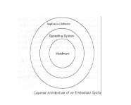
Figure 2.1: Embedded Layer Architecture
The operating system runs above the hardware, and the application software runs above the operating system. The same architecture is applicable to any computer including a desktop computer. However, there are significant differences. It is not compulsory to have an operating system in every embedded system. For small appliances such as remote control units, air conditioners, toys etc., there is no need for an operating system and you can write only the software specific to that application. For applications involving complex processing, it is advisable to have an operating system. In such a case, you need to integrate the application software with the operating system and then transfer the entire software on to the memory chip. Once the software is transferred to the memory chip, the software will continue to run for a long time you don’t need to reload new software.
Now, let us see the details of the various building blocks of the hardware of an embedded system. As shown in Fig. the building blocks are;
- Central Processing Unit (CPU)
- Memory (Read-only Memory and Random Access Memory)
- Input Devices
- Output devices
- Communication interfaces
- Application-specific circuitry
Central Processing Unit (CPU):
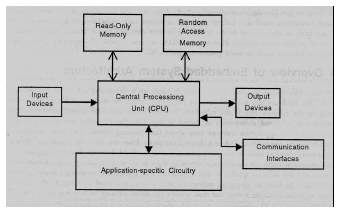
Figure 2.2: Embedded Architecture
The Central Processing Unit (processor, in short) can be any of the following: microcontroller, microprocessor or Digital Signal Processor (DSP). A micro-controller is a low-cost processor. Its main attraction is that on the chip itself, there will be many other components such as memory, serial communication interface, analog-to digital converter etc. So, for small applications, a micro-controller is the best choice as the number of external components required will be very less. On the other hand, microprocessors are more powerful, but you need to use many external components with them. D5P is used mainly for applications in which signal processing is involved such as audio and video processing.
Memory:
The memory is categorized as Random Access 11emory (RAM) and Read Only Memory (ROM). The contents of the RAM will be erased if power is switched off to the chip, whereas ROM retains the contents even if the power is switched off. So, the firmware is stored in the ROM. When power is switched on, the processor reads the ROM; the program is program is executed.
Input devices:
Unlike the desktops, the input devices to an embedded system have very limited capability. There will be no keyboard or a mouse, and hence interacting with the embedded system is no easy task. Many embedded systems will have a small keypad-you press one key to give a specific command. A keypad may be used to input only the digits. Many embedded systems used in process control do not have any input device for user interaction; they take inputs from sensors or transducers 1’fnd produce electrical signals that are in turn fed to other systems.
Output devices:
The output devices of the embedded systems also have very limited capability. Some embedded systems will have a few Light Emitting Diodes (LEDs) to indicate the health status of the system modules, or for visual indication of alarms. A small Liquid Crystal Display (LCD) may also be used to display some important parameters.
Communication interfaces:
The embedded systems may need to, interact with other embedded systems at they may have to transmit data to a desktop. To facilitate this, the embedded systems are provided with one or a few communication interfaces such as RS232, RS422, RS485, Universal Serial Bus (USB), IEEE 1394, Ethernet etc.
Application-specific circuitry:
Sensors, transducers, special processing and control circuitry may be required fat an embedded system, depending on its application. This circuitry interacts with the processor to carry out the necessary work. The entire hardware has to be given power supply either through the 230 volts main supply or through a battery. The hardware has to design in such a way that the power consumption is minimized.
CHAPTER 3: HARDWARE IMPLEMENTATION OF THE PROJECT
This chapter briefly explains about the Hardware Implementation of the project. It discusses the design and working of the design with the help of block diagram in detail. It explains the features, timer programming, serial communication, interrupts of 8051 microcontroller. It also explains the various modules used in this project.
3.1 Project Design
The implementation of the project design can be divided in two parts.
- Hardware implementation
- Firmware implementation
Hardware implementation deals in drawing the schematic on the plane paper according to the application, testing the schematic design over the breadboard using the various IC’s to find if the design meets the objective, carrying out the PCB layout of the schematic tested on breadboard, finally preparing the board and testing the designed hardware.
The firmware part deals in programming the microcontroller so that it can control the operation of the IC’s used in the implementation. In the present work, we have used the Orcad design software for PCB circuit design, the Keil µv3 software development tool to write and compile the source code, which has been written in the C language. The Proload programmer has been used to write this compile code into the microcontroller. The firmware implementation is explained in the next chapter.
The project design and principle are explained in this chapter using the block diagram and circuit diagram. The block diagram discusses about the required components of the design and working condition is explained using circuit diagram and system wiring diagram.
3.1.1 Block Diagram of the Project and its Description
The block diagram of the design is as shown in Fig 3.1. It consists of power supply unit, 8051 microcontroller, GSM, LCD Display,MAX232, TRIAC, Loads and Feedback circuit . The brief description of each unit is explained as follows.
Block diagram:
µC
KEY PAD


LCD DISPLAY
POWERSUPPLY


RFID READER

GSM MODULE
Figure 3.1: Block Diagram
3.1. POWER SUPPLY
33330Ω
3.3. MICROCONTROLLER (8052)
Microprocessors and microcontrollers are widely used in embedded systems products. Microcontroller is a programmable device. A microcontroller has a CPU in addition to a fixed amount of RAM, ROM, I/O ports and a timer embedded all on a single chip. The fixed amount of on-chip ROM, RAM and number of I/O ports in microcontrollers makes them ideal for many applications in which cost and space are critical.
The Intel 8052 is Harvard architecture, single chip microcontroller (µC) which was developed by Intel in 1980 for use in embedded systems. It was popular in the 1980s and early 1990s, but today it has largely been superseded by a vast range of enhanced devices with 8051-compatible processor cores that are manufactured by more than 20 independent manufacturers including Atmel, Infineon Technologies and Maxim Integrated Products.
8052 is an 8-bit processor, meaning that the CPU can work on only 8 bits of data at a time. Data larger than 8 bits has to be broken into 8-bit pieces to be processed by the CPU. 8052 is available in different memory types such as UV-EPROM, Flash and NV-RAM.
Features of AT89S52:
- 8K Bytes of Re-programmable Flash Memory
- RAM is 256 bytes
- 4.0V to 5.5V Operating Range
- Fully Static Operation: 0 Hz to 33 MHz’s
- Three-level Program Memory Lock
- 256 x 8-bit Internal RAM
- 32 Programmable I/O Lines
- Three 16-bit Timer/Counters
- Eight Interrupt Sources
- Full Duplex UART Serial Channel
- Low-power Idle and Power-down Modes
- Interrupt recovery from power down mode
- Watchdog timer
- Dual data pointer
- Power-off flag
- Fast programming time
- Flexible ISP programming (byte and page mode)
Description:
The AT89s52 is a low-voltage, high-performance CMOS 8-bit microcomputer with 8K bytes of Flash programmable memory. The device is manufactured using Atmel’s high density nonvolatile memory technology and is compatible with the industry-standard MCS-51 instruction set. The on chip flash allows the program memory to be reprogrammed in system or by a conventional non volatile memory programmer. By combining a versatile 8-bit CPU with Flash on a monolithic chip, the Atmel AT89s52 is a powerful microcomputer, which provides a highly flexible and cost-effective solution to many embedded control applications.
In addition, the AT89s52 is designed with static logic for operation down to zero frequency and supports two software selectable power saving modes. The Idle Mode stops the CPU while allowing the RAM, timer/counters, serial port and interrupt system to continue functioning. The power-down mode saves the RAM contents but freezes the oscillator disabling all other chip functions until the next hardware reset.
Pin diagram:
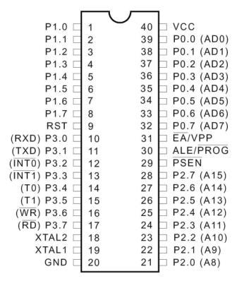
Figure 3.4: Pin Diagram of 8052
Pin description:
Vcc Pin 40 provides supply voltage to the chip. The voltage source is +5V.
GND Pin 20 is the ground.
Port 0:
Port 0 is an 8-bit open drain bidirectional I/O port. As an output port, each pin can sink eight TTL inputs. When 1s are written to port 0 pins, the pins can be used as high impedance inputs. Port 0 can also be configured to be the multiplexed low-order address/data bus during accesses to external program and data memory. In this mode, P0 has internal pull-ups.
Port 0 also receives the code bytes during Flash programming and outputs the code bytes during Program verification. External pull-ups are required during program verification.
Port 1:
Port 1 is an 8-bit bidirectional I/O port with internal pull-ups. The Port 1 output buffers can sink/source four TTL inputs. When 1s are written to Port 1 pins, they are pulled high by the internal pull-ups and can be used as inputs. As inputs, Port 1 pins that are externally being pulled low will source current (IIL) because of the internal pull-ups. In addition, P1.0 and P1.1 can be configured to be the timer/counter 2 external count input (P1.0/T2) and the timer/counter 2 trigger input (P1.1/T2EX), respectively, as shown in the following table.
Port 1 also receives the low-order address bytes during Flash programming and verification.
Port 2:
Port 2 is an 8-bit bidirectional I/O port with internal pull-ups. The Port 2 output buffers can sink/source four TTL inputs. When 1s are written to Port 2 pins, they are pulled high by the internal pull-ups and can be used as inputs. As inputs, Port 2 pins that are externally being pulled low will source current (IIL) because of the internal pull-ups.
Port 2 emits the high-order address byte during fetches from external program memory and during accesses to external data memory that uses 16-bit addresses (MOVX @ DPTR). In this application, Port 2 uses strong internal pull-ups when emitting 1s. During accesses to external data memory that uses 8-bit addresses (MOVX @ RI), Port 2 emits the contents of the P2 Special Function Register. The port also receives the high-order address bits and some control signals during Flash programming and verification.
Port 3:
Port 3 is an 8-bit bidirectional I/O port with internal pull-ups. The Port 3 output buffers can sink/source four TTL inputs. When 1s are written to Port 3 pins, they are pulled high by the internal pull-ups and can be used as inputs. As inputs, Port 3 pins that are externally being pulled low will source current (IIL) because of the pull-ups. Port 3 receives some control signals for Flash programming and verification.
Port 3 also serves the functions of various special features of the AT89S52, as shown in the following table.
RST:
Reset input A high on this pin for two machine cycles while the oscillator is running resets the device. This pin drives high for 98 oscillator periods after the Watchdog times out. The DISRTO bit in SFR AUXR (address 8EH) can be used to disable this feature. In the default state of bit DISRTO, the RESET HIGH out feature is enabled.
ALE/PROG:
Address Latch Enable (ALE) is an output pulse for latching the low byte of the address during accesses to external memory. This pin is also the program pulse input (PROG) during Flash programming.
In normal operation, ALE is emitted at a constant rate of 1/6 the oscillator frequency and may be used for external timing or clocking purposes. Note, however, that one ALE pulse is skipped during each access to external data memory.
If desired, ALE operation can be disabled by setting bit 0 of SFR location 8EH. With the bit set, ALE is active only during a MOVX or MOVC instruction. Otherwise, the pin is weakly pulled high. Setting the ALE-disable bit has no effect if the microcontroller is in external execution mode.
PSEN:
Program Store Enable (PSEN) is the read strobe to external program memory. When the AT89S52 is executing code from external program memory, PSEN is activated twice each machine cycle, except that two PSEN activations are skipped during each access to external data memory.
EA/VPP:
External Access Enable EA must be strapped to GND in order to enable the device to fetch code from external program memory locations starting at 0000H up to FFFFH. Note, however, that if lock bit 1 is programmed, EA will be internally latched on reset.
EA should be strapped to VCC for internal program executions. This pin also receives the 12-volt programming enable voltage (VPP) during Flash programming.
XTAL1:
Input to the inverting oscillator amplifier and input to the internal clock operating circuit.
XTAL2:
Output from the inverting oscillator amplifier.
XTAL1 and XTAL2 are the input and output, respectively, of an inverting amplifier that can be configured for use as an on-chip oscillator. Either a quartz crystal or ceramic resonator may be used. To drive the device from an external clock source, XTAL2 should be left unconnected while XTAL1 is driven. There are no requirements on the duty cycle of the external clock signal, since the input to the internal clocking circuitry is through a divide-by-two flip-flop, but minimum and maximum voltage high and low time specifications must be observed.
Special Function Registers:
A map of the on-chip memory area called the Special Function Register (SFR) space is shown in the following table.
It should be noted that not all of the addresses are occupied and unoccupied addresses may not be implemented on the chip. Read accesses to these addresses will in general return random data, and write accesses will have an indeterminate effect.
User software should not write 1s to these unlisted locations, since they may be used in future products to invoke new features. In that case, the reset or inactive values of the new bits will always be 0.
Timer 2 Registers:
Control and status bits are contained in registers T2CON and T2MOD for Timer 2. The register pair (RCAP2H, RCAP2L) is the Capture/Reload register for Timer 2 in 16-bit capture mode or 16-bit auto-reload mode.
Interrupt Registers:
The individual interrupt enable bits are in the IE register. Two priorities can be set for each of the six interrupt sources in the IP register.
Dual Data Pointer Registers:
To facilitate accessing both internal and external data memory, two banks of 16-bit Data Pointer Registers are provided: DP0 at SFR address locations 82H-83H and DP1 at 84H and 85H. Bit DPS = 0 in SFR AUXR1 selects DP0 and DPS = 1 selects DP1. The user should ALWAYS initialize the DPS bit to the appropriate value before accessing the respective Data Pointer Register.
Power off Flag:
The Power off Flag (POF) is located at bit 4 (PCON.4) in the PCON SFR. POF is set to “1” during power up. It can be set and rest under software control and is not affected by reset.
Memory Organization
MCS-51 devices have a separate address space for Program and Data Memory. Up to 64K bytes each of external Program and Data Memory can be addressed.
Program Memory:
If the EA pin is connected to GND, all program fetches are directed to external memory. On the AT89S52, if EA is connected to VCC, program fetches to addresses 0000H through 1FFFH are directed to internal memory and fetches to addresses 2000H through FFFFH are to external memory.
Data Memory:
The AT89S52 implements 256 bytes of on-chip RAM. The upper 128 bytes occupy a parallel address space to the Special Function Registers. This means that the upper 128 bytes have the same addresses as the SFR space but are physically separate from SFR space.
When an instruction accesses an internal location above address 7FH, the address mode used in the instruction specifies whether the CPU accesses the upper 128 bytes of RAM or the SFR space. Instructions which use direct addressing access the SFR space.
For example, the following direct addressing instruction accesses the SFR at location 0A0H (which is P2).
MOV 0A0H, #data
The instructions that use indirect addressing access the upper 128 bytes of RAM. For example, the following indirect addressing instruction, where R0 contains 0A0H, accesses the data byte at address 0A0H, rather than P2 (whose address is 0A0H).
MOV @R0, #data
It should be noted that stack operations are examples of indirect addressing, so the upper 128 bytes of data RAM are available as stack space.
Watchdog Timer (One-time Enabled with Reset-out)
The WDT is intended as a recovery method in situations where the CPU may be subjected to software upsets. The WDT consists of a 14-bit counter and the Watchdog Timer Reset (WDTRST) SFR. The WDT is defaulted to disable from exiting reset. To enable the WDT, a user must write 01EH and 0E1H in sequence to the WDTRST register (SFR location 0A6H).
When the WDT is enabled, it will increment every machine cycle while the oscillator is running. The WDT timeout period is dependent on the external clock frequency. There is no way to disable the WDT except through reset (either hardware reset or WDT overflow reset). When WDT overflows, it will drive an output RESET HIGH pulse at the RST pin.
UART:
The Atmel 8052 Microcontrollers implement three general purpose, 16-bit timers/ counters. They are identified as Timer 0, Timer 1 and Timer 2 and can be independently configured to operate in a variety of modes as a timer or as an event counter. When operating as a timer, the timer/counter runs for a programmed length of time and then issues an interrupt request. When operating as a counter, the timer/counter counts negative transitions on an external pin. After a preset number of counts, the counter issues an interrupt request. The various operating modes of each timer/counter are described in the following sections.
A basic operation consists of timer registers THx and TLx (x= 0, 1) connected in cascade to form a 16-bit timer. Setting the run control bit (TRx) in TCON register turns the timer on by allowing the selected input to increment TLx. When TLx overflows it increments THx; when THx overflows it sets the timer overflow flag (TFx) in TCON register. Setting the TRx does not clear the THx and TLx timer registers. Timer registers can be accessed to obtain the current count or to enter preset values. They can be read at any time but TRx bit must be cleared to preset their values, otherwise the behavior of the timer/counter is unpredictable.
The C/T control bit (in TCON register) selects timer operation or counter operation, by selecting the divided-down peripheral clock or external pin Tx as the source for the counted signal. TRx bit must be cleared when changing the mode of operation, otherwise the behavior of the timer/counter is unpredictable. For timer operation (C/Tx# = 0), the timer register counts the divided-down peripheral clock. The timer register is incremented once every peripheral cycle (6 peripheral clock periods). The timer clock rate is FPER / 6, i.e. FOSC / 12 in standard mode or FOSC / 6 in X2 mode. For counter operation (C/Tx# = 1), the timer register counts the negative transitions on the Tx external input pin. The external input is sampled every peripheral cycle. When the sample is high in one cycle and low in the next one, the counter is incremented.
Since it takes 2 cycles (12 peripheral clock periods) to recognize a negative transition, the maximum count rate is FPER / 12, i.e. FOSC / 24 in standard mode or FOSC / 12 in X2 mode. There are no restrictions on the duty cycle of the external input signal, but to ensure that a given level is sampled at least once before it changes, it should be held for at least one full peripheral cycle. In addition to the “timer” or “counter” selection, Timer 0 and Timer 1 have four operating modes from which to select which are selected by bit-pairs (M1, M0) in TMOD. Modes 0, 1and 2 are the same for both timer/counters. Mode 3 is different.
The four operating modes are described below. Timer 2, has three modes of operation: ‘capture’, ‘auto-reload’ and ‘baud rate generator’.
Timer 0:
Timer 0 functions as either a timer or event counter in four modes of operation. Timer 0 is controlled by the four lower bits of the TMOD register and bits 0, 1, 4 and 5 of the TCON register. TMOD register selects the method of timer gating (GATE0), timer or counter operation (T/C0#) and mode of operation (M10 and M00). The TCON register provides timer 0 control functions: overflow flag (TF0), run control bit (TR0), interrupt flag (IE0) and interrupt type control bit (IT0).
For normal timer operation (GATE0= 0), setting TR0 allows TL0 to be incremented by the selected input. Setting GATE0 and TR0 allows external pin INT0# to control timer operation.
Timer 0 overflow (count rolls over from all 1s to all 0s) sets TF0 flag, generating an interrupt request. It is important to stop timer/counter before changing mode.
Mode 0 (13-bit Timer):
Mode 0 configures timer 0 as a 13-bit timer which is set up as an 8-bit timer (TH0 register) with a modulo-32 prescaler implemented with the lower five bits of the TL0 register. The upper three bits of TL0 register are indeterminate and should be ignored. Prescaler overflow increments the TH0 register.
As the count rolls over from all 1’s to all 0’s, it sets the timer interrupt flag TF0. The counted input is enabled to the Timer when TR0 = 1 and either GATE = 0 or INT0 = 1. (Setting GATE = 1 allows the Timer to be controlled by external input INT0, to facilitate pulse width measurements). TR0 is a control bit in the Special Function register TCON. GATE is in TMOD.
The 13-bit register consists of all 8 bits of TH0 and the lower 5 bits of TL0. The upper 3 bits of TL0 are indeterminate and should be ignored. Setting the run flag (TR0) does not clear the registers.
Mode 0 operation is the same for Timer 0 as for Timer 1. There are two different GATE bits, one for Timer 1 (TMOD.7) and one for Timer 0 (TMOD.3).
Baud Rate Generator:
Timer 2 is selected as the baud rate generator by setting TCLK and/or RCLK in T2CON. Note that the baud rates for transmit and receive can be different if Timer 2 is used for the receiver or transmitter and Timer 1 is used for the other function. Setting RCLK and/or TCLK puts Timer 2 into its baud rate generator mode.
The baud rate generator mode is similar to the auto-reload mode, in that a rollover in TH2 causes the Timer 2 registers to be reloaded with the 16-bit value in registers RCAP2H and RCAP2L, which are preset by software.
The baud rates in Modes 1 and 3 are determined by Timer 2’s overflow rate according to the following equation.
The Timer can be configured for either timer or counter operation. In most applications, it is configured for timer operation (CP/T2 = 0). The timer operation is different for Timer 2 when it is used as a baud rate generator. Normally, as a timer, it increments every machine cycle (at 1/12 the oscillator frequency). As a baud rate generator, however, it increments every state time (at 1/2 the oscillator frequency). The baud rate formula is given below where (RCAP2H, RCAP2L) is the content of RCAP2H and RCAP2L taken as a 16-bit unsigned integer.
Timer 2 as a baud rate generator is shown in the below figure. This figure is valid only if RCLK or TCLK = 1 in T2CON. Note that a rollover in TH2 does not set TF2 and will not generate an interrupt. Note too, that if EXEN2 is set, a 1-to-0 transition in T2EX will set EXF2 but will not cause a reload from (RCAP2H, RCAP2L) to (TH2, TL2). Thus, when Timer 2 is in use as a baud rate generator, T2EX can be used as an extra external interrupt.
It should be noted that when Timer 2 is running (TR2 = 1) as a timer in the baud rate generator mode, TH2 or TL2 should not be read from or written to. Under these conditions, the Timer is incremented every state time, and the results of a read or write may not be accurate. The RCAP2 registers may be read but should not be written to, because a write might overlap a reload and cause write and/or reload errors. The timer should be turned off (clear TR2) before accessing the Timer 2 or RCAP2 registers.
Interrupts:
The AT89S52 has a total of six interrupt vectors: two external interrupts (INT0 and INT1), three timer interrupts (Timers 0, 1, and 2) and the serial port interrupt. These interrupts are all shown in the below figure.
Each of these interrupt sources can be individually enabled or disabled by setting or clearing a bit in Special Function Register IE. IE also contains a global disable bit, EA, which disables all interrupts at once. The below table shows that bit position IE.6 is unimplemented. User software should not write a 1 to this bit position, since it may be used in future AT89 products.
Timer 2 interrupt is generated by the logical OR of bits TF2 and EXF2 in register T2CON. Neither of these flags is cleared by hardware when the service routine is vectored to. In fact, the service routine may have to determine whether it was TF2 or EXF2 that generated the interrupt, and that bit will have to be cleared in software.
The Timer 0 and Timer 1 flags, TF0 and TF1, are set at S5P2 of the cycle in which the timers overflow. The values are then polled by the circuitry in the next cycle. However, the Timer 2 flag, TF2, is set at S2P2 and is polled in the same cycle in which the timer overflows.
CRYSTAL OSCILLATOR:
The 8052 uses the crystal for precisely that: to synchronize it’s operation. Effectively, the 8052 operates using what are called “machine cycles.” A single machine cycle is the minimum amount of time in which a single 8052 instruction can be executed. Although many instructions take multiple cycles. 8052 has an on-chip oscillator. It needs an external crystal that decides the operating frequency of the 8052. The crystal is connected to pins 18 and 19 with stabilizing capacitors. 12 MHz (11.059MHz) crystal is often used and the capacitance ranges from 20pF to 40pF.
A cycle is, in reality, 12 pulses of the crystal. That is to say, if an instruction takes one machine cycle to execute, it will take 12 pulses of the crystal to execute. Since we know the we can calculate how many instruction cycles the 8052 can execute per second:
11,059,000 / 12 = 921,583
11.0592 MHz crystals are often used because it can be divided to give you exact clock rates for most of the common baud rates for the UART, especially for the higher speeds (9600, 19200).
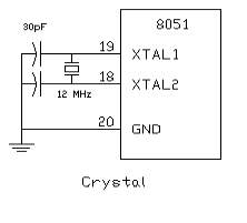
Figure 3.5: Crystal Oscillator Circuit
RESET:
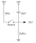
Figure 3.6: RESET Pin Circuit
RESET is an active High input When RESET is set to High, 8052 goes back to the power on state. The 8052 is reset by holding the RST high for at least two machine cycles and then returning it low. Initially charging of capacitor makes RST High, When capacitor charges fully it blocks DC.
SIP Resistor:
Sip Resistor is a single in pack Resistor (i.e.,) 8 resistors connected in series. Basically SIP resistor is a 9 pin connector first pin is for power supply to the entire 8 resistors in SIP.
Generally SIP Resistor is used to close the open drain connections of Port 0.
3.4. RFID Reader:
Figure 3.7: RFID Reader
Radio Frequency Identification (RFID) Card Readers provide a low-cost solution to read passive RFID transponder tags up to 7 cm away. This RFID Card Reader can be used in a wide variety of hobbyist and commercial applications, including access control, automatic identification, robotics navigation, inventory tracking, payment systems, and car immobilization. The RFID card reader read the RFID tag in range and outputs unique identification code of the tag at baud rate of 9600. The data from RFID reader can be interfaced to be read by microcontroller or PC.
Radio-frequency identification (RFID) is an automatic identification method, relying on storing and remotely retrieving data using devices called RFID tags or transponders. The technology requires some extent of cooperation of an RFID reader and an RFID tag. An RFID tag is an object that can be applied to or incorporated into a product, animal, or person for the purpose of identification and tracking using radio waves. Some tags can be read from several meters away and beyond the line of sight of the reader.
An RFID tag is an object that can be applied to or incorporated into a product, animal, or person for the purpose of identification and tracking using radio waves. Some tags can be read from several meters away and beyond the line of sight of the reader.
What is RFID?
A basic RFID system consists of three components:
a) An antenna or coil
b) A transceiver (with decoder)
c) A transponder (RF tag)
Electronically programmed with unique information. There are many different types of RFID systems out in the market. They are categorized according to their frequency ranges. Some of the most commonly used RFID kits are as follows:
- Low-frequency (30 KHz to 500 KHz)
- Mid-Frequency (900KHz to 1500MHz)
- High Frequency (2.4GHz to 2.5GHz)
These frequency ranges mostly tell the RF ranges of the tags from low frequency tag ranging from 3m to 5m, mid frequency ranging from 5m to 17m and high frequency ranging from 5ft to 90ft. The cost of the system is based according to their ranges with low-frequency system ranging from a few hundred dollars to a high-frequency system ranging somewhere near 5000 dollars.
Radio Frequency Identification (RFID) Card Readers provide a low-cost solution to read passive RFID transponder tags up to 2 inches away. The RFID Card Readers can be used in a wide variety of hobbyist and commercial applications, including access control, automatic identification, robotics navigation, inventory tracking, payment systems, and car immobilization. The RFID card reader read the RFID tag in range and outputs unique identification code of the tag at baud rate of 9600. The data from RFID reader can be interfaced to be read by microcontroller or PC.
Features:
- Low-cost method for reading passive RFID transponder tags
- 9600 bps serial interface at RS232 level
- Buzzer & LED indicate valid RFID Tag detection
- RS232 interface connects directly to PC, Mac or Linux machine and requires no additional wiring.
RFID Reader Package Includes:
RFID Reader (Assembled & Tested with 1 year warranty)
Serial Cable
Information:
Each transponder tag contains a unique identifier (one of 240, or 1,099,511,627,776 possible combinations) that is read by the RFID Card Reader and transmitted to the host via a simple serial interface. It means no two tags are same. Each tag has different value. This value if read by reader.
Communication:
When the RFID Card Reader is active and a valid RFID transponder tag is placed within range of the activated reader, the unique ID will be transmitted as a 12-byte printable ASCII string serially to the host in the following format:
The start byte and stop byte are used to easily identify that a correct string has been received from the reader (they correspond to a line feed and carriage return characters, respectively). The middle ten bytes are the actual tag’s unique ID. For example, for a tag with a valid ID of 0F0184F07A, the following ASCII data would be sent 0F0184F07A Same data in HEX bytes can be interpreted as: 0x0A, 0x30, 0x46, 0x30, 0x31, 0x38, 0x34, 0x46, 0x30, 0x37, 0x41, 0x0D All communication is 8 data bits, no parity, 1 stop bit, and least significant bit first (8N1). The baud rate is configured for 9600 bps, a standard communications speed supported by most any microprocessor or PC, and cannot be changed. The RFID Card Reader initiates all communication. This allows easy access to the serial data stream from any programming language that can open a COM port.
Using RFID Reader:
When powered on the RFID reader will activate a RF field waiting for a tag to come into its range. Once tag is detected, its unique ID number is read and data is sent via serial interface. The valid tag detecting is indicated by LED blink and Buzzer beep. The face of the RFID tag should be held parallel to the front of the antenna (where the majority of RF energy is focused). If the tag is held sideways (perpendicular to the antenna) you may have difficulty getting the tag to be read. Only one transponder tag should be held up to the antenna at any time. The use of multiple tags at one time will cause tag collisions and confuse the reader. The tags available with us have a read distance of approximately 2 inches. Actual distance may vary slightly depending on the size of the transponder tag and environmental conditions of the application. On PC you can use software like hyper terminal which can show ASCII data at 9600 baud rate. You can also develop software in any language which can connect to serial port and listen for incoming ASCII data.
Power Requirement of Receiver:
The unit needs around 200mA power to operate at 12V. You can use any readymade 12V 500mA DC Adapter or design a transformer plus rectifier based 12V DC power for the board. You can also use just the 12V transformer as the board has bridge and capacitor to convert to DC. We recommend SMPS based 12V 1A DC Adapter for 24 hours operation as it is efficient and does not generate heat as compared to transformer based adapters. Serial Cable connections for RS232 interfacing (Provided with product) To use with a PC serial port, use a serial cable of male-female type with pins 2,3,5 connected to 2,3,5 straight(no cross over cable).

Figure 3.8: RFID Power requirement
Connecting to PC:
Use the supplied serial cable to connect to PC’s serial port. Use Hyperterminal software which comes with Windows XP or use any other Terminal software with following settings.
Data Rate: 9600 Data Bits: 8 Parity: None Stop Bit: 1 Flow Control: None
RFID Technology Overview:
Radio Frequency Identification (RFID) is a generic term for non-contacting technologies that use radio waves to automatically identify people or objects. There are several methods of identification, but the most common is to store a unique serial number that identifies a person or object on a microchip that is attached to an antenna. The combined antenna and microchip are called an “RFID transponder” or “RFID tag” and work in combination with an “RFID reader” (sometimes called an “RFID interrogator”). An RFID system consists of a reader and one or more tags. The reader’s antenna is used to transmit radio frequency (RF) energy. Depending on the tag type, the energy is “harvested” by the tag’s antenna and used to power up the internal circuitry of the tag. The tag will then modulate the electromagnetic waves generated by the reader in order to transmit its data back to the reader. The reader receives the modulated waves and converts them into digital data. There are two major types of tag technologies. “Passive tags” are tags that do not contain their own power source or transmitter. When radio waves from the reader reach the chip’s antenna, the energy is converted by the antenna into electricity that can power up the microchip in the tag (known as “parasitic power”). The tag is then able to send back any information stored on the tag by reflecting the electromagnetic waves as described above. “Active tags” have their own power source and transmitter.
The power source, usually a battery, is used to run the microchip’s circuitry and to broadcast a signal to a reader. Due to the fact that passive tags do not have their own transmitter and must reflect their signal to the reader, the reading distance is much shorter than with active tags. However, active tags are typically larger, more expensive, and require occasional service. The RFID Card Reader is designed specifically for passive tags. Frequency refers to the size of the radio waves used to communicate between the RFID system components. Just as you tune your radio to different frequencies in order to hear different radio stations, RFID tags and readers must be tuned to the same frequency in order to communicate effectively. There really is no such thing as a “typical” RFID tag. The read range of a tag ultimately depends on many factors: the frequency of RFID system operation, the power of the reader, environmental conditions, physical size of the tags antenna and interference from other RF devices. Balancing a number of engineering trade-offs (antenna size v. reading distance v. power v. manufacturing cost), the Sunrom RFID Card Reader’s antenna was designed with a RFID operation at a tag read distance of around 4 inches.
COMPONENTS OF RFID:
A basic RFID system consist of three components:
- An antenna or coil
- A transceiver (with decoder)
- A transponder (RF tag) electronically programmed with unique information
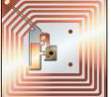
1. ANTENNA:
The antenna emits radio signals to activate the tag and read and write data to it. Antennas are the conduits between the tag and the transceiver, which controls the system’s data acquisition and communication. Antennas are available in a variety of shapes and sizes; they can be built into a door frame to receive tag data from persons or things passing through the door, or mounted on an interstate tollbooth to monitor traffic passing by on a freeway. The electromagnetic field produced by an antenna can be constantly present when multiple tags are expected continually. If constant interrogation is not required, a sensor device can activate the field. Often the antenna is packaged with the transceiver and decoder to become a reader (a.k.a. interrogator), which can be configured either as a handheld or a fixed-mount device.
The reader emits radio waves in ranges of anywhere from one inch to 100 feet or more, depending upon its power output and the radio frequency used. When an RFID tag passes through the electromagnetic zone, it detects the reader’s activation signal. The reader decodes the data encoded in the tag’s integrated circuit (silicon chip) and the data is passed to the host computer for processing.
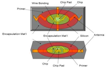
Figure 3.9: RFID Antenna
2. TAGS (Transponders):
An RFID tag is comprised of a microchip containing identifying information and an antenna that transmits this data wirelessly to a reader. At its most basic, the chip will contain a serialized identifier, or license plate number, that uniquely identifies that item, similar to the way many bar codes are used today. A key difference, however is that RFID tags have a higher data capacity than their bar code counterparts. This increases the options for the type of information that can be encoded on the tag, including the manufacturer, batch or lot number, weight, ownership, destination and history (such as the temperature range to which an item has been exposed). In fact, an unlimited list of other types of information can be stored on RFID tags, depending on application needs. An RFID tag can be placed on individual items, cases or pallets for identification purposes, as well as on fixed assets such as trailers, containers, totes, etc Tags come in a variety of types, with a variety of capabilities. Key variables include: “Read-only” versus “read-write” There are three options in terms of how data can be encoded on tags: (1) Read-only tags contain data such as a serialized tracking number, which is pre-written onto them
by the tag manufacturer or distributor. These are generally the least expensive tags because they cannot have any additional information included as they move throughout the supply chain. Any updates to that information would have to be maintained in the application software that tracks SKU movement and activity. (2) “Write once” tags enable a user to write data to the tag one time in production or distribution processes. Again, this may include a serial number, but perhaps other data such as a lot or batch number. (3) Full “read-write” tags allow new data to be written to the tag as needed and even written over the original data. Examples for the latter capability might include the time and date of ownership transfer or updating the repair history of a fixed asset. While these are the most costly of the three tag types and are not practical for tracking inexpensive items, future standards for electronic product codes (EPC) appear to be headed in this direction.
RFID TAGS
Figure 3.10: RFID Tag
DATA CAPACITY:
The amount of data storage on a tag can vary, ranging from 16 bits on the low end to as much as several thousand bits on the high end. Of course, the greater the storage capacity, the higher the price per tag.
FORM FACTOR:
The tag and antenna structure can come in a variety of physical form factors and can either be self-contained or embedded as part of a traditional label structure (i.e., the tag is inside what looks like a regular bar code label this is termed a ‘Smart Label’) companies must choose the appropriate form factors for the tag very carefully and should expect to use multiple form factors to suit the tagging needs of different physical products and units of measure. For example, a pallet may have an RFID tag fitted only to an area of protected placement on the pallet itself. On the other hand, cartons on the pallet have RFID tags inside bar code labels that also provide operators human readable information and a back-up should the tag fail or pass through non RFID-capable supply chain links.
FREQUENCIES:
Like all wireless communications, there are a variety of frequencies or spectra through which RFID tags can communicate with readers. Again, there are trade-offs among cost, performance and application requirements. For instance, low-frequency tags are cheaper than ultra high frequency (UHF) tags, use less power and are better able to penetrate non-metallic substances. They are ideal for scanning objects with high water content, such as fruit, at close range. UHF frequencies typically offer better range and can transfer data faster. But they use more power and are less likely to pass through some materials. UHF tags are typically best suited for use with or near wood, paper, cardboard or clothing products. Compared to low frequency tags, UHF tags might be better for scanning boxes of goods as they pass through a bay door into a warehouse. While the tag requirements for compliance mandates may be narrowly defined, it is likely that a variety of tag types will be required to solve specific operational issues. You will want to work with a company that is very knowledgeable in tag and reader technology to appropriately identify the right mix of RFID technology for your environment and applications.
EPC TAGS:
EPC refers to “electronic product code,” an emerging specification for RFID tags, readers and business applications first developed at the Auto-ID Center at the Massachusetts Institute of Technology. This organization has provided significant intellectual leadership toward the use and application of RFID technology. EPC represents a specific approach to item identification, including an emerging standard for the tags themselves, including both the data content of the tag and open wireless communication protocols. In a sense, the EPC movement is combining the data standards embodied in certain bar code specifications, such as the UPC or UCC-128 bar code standards, with the wireless data communication standards that have been developed by ANSI and other groups.
3. RF TRANSCEIVER:
The RF transceiver is the source of the RF energy used to activate and power the passive RFID tags. The RF transceiver may be enclosed in the same cabinet as the reader or it may be a separate piece of equipment. When provided as a separate piece of equipment, the transceiver is commonly referred to as an RF module. The RF transceiver controls and modulates the radio frequencies that the antenna transmits and receives. The transceiver filters and amplifies the backscatter signal from a passive RFID tag.
Typical Applications for RFID:
- Automatic Vehicle identification
- Inventory Management
- Work-in-Process
- Container/ Yard Management
- Document/ Jewellery tracking
- Patient Monitoring
The Advantages of RFID Over Bar Coding:
- No “line of sight” requirements: Bar code reads can sometimes be limited or problematic due to the need to have a direct “line of sight” between a scanner and a bar code. RFID tags can be read through materials without line of sight.
- More automated reading: RFID tags can be read automatically when a tagged product comes past or near a reader, reducing the labor required to scan product and allowing more proactive, realtime tracking.
- Improved read rates: RFID tags ultimately offer the promise of higher read rates than bar codes, especially in high-speed operations such as carton sortation.
- Greater data capacity: RFID tags can be easily encoded with item details such as lot and batch, weight, etc.
- “Write” capabilities: Because RFID tags can be rewritten with new data as supply chain activities are completed, tagged products carry updated information as they move throughout the supply chain.
Common Problems with RFID:
Some common problems with RFID are reader collision and tag collision. Reader collision occurs when the signals from two or more readers overlap. The tag is unable to respond to simultaneous queries. Systems must be carefully set up to avoid this problem. Tag collision occurs when many tags are present in a small area; but since the read time is very fast, it is easier for vendors to develop systems that ensure that tags respond one at a time. See Problems with RFID for more details.
3.5. MAX 232:
Max232 IC is a specialized circuit which makes standard voltages as required by RS232 standards. This IC provides best noise rejection and very reliable against discharges and short circuits. MAX232 IC chips are commonly referred to as line drivers.
Figure 3.11: MAX232 IC
To ensure data transfer between PC and microcontroller, the baud rate and voltage levels of Microcontroller and PC should be the same. The voltage levels of microcontroller are logic1 and logic 0 i.e., logic 1 is +5V and logic 0 is 0V. But for PC, RS232 voltage levels are considered and they are: logic 1 is taken as -3V to -25V and logic 0 as +3V to +25V. So, in order to equal these voltage levels, MAX232 IC is used. Thus this IC converts RS232 voltage levels to microcontroller voltage levels and vice versa.
Pin Configuration and Functions:
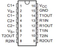
Figure 3.12: MAX 232 Pin diagram
Pin Description:
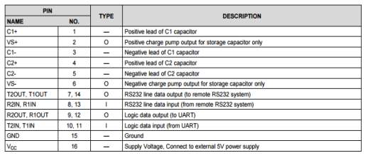
Table 3.1:MAX232 Pin description
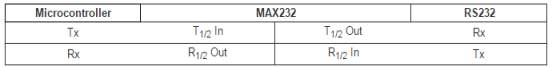
The MAX232 IC is used to convert the TTL/CMOS logic levels to RS232 logic levels during serial communication of microcontrollers with PC. The controller operates at TTL logic level (0-5V) whereas the serial communication in PC works on RS232 standards (-25 V to + 25V). This makes it difficult to establish a direct link between them to communicate with each other.
The intermediate link is provided through MAX232. It is a dual driver/receiver that includes a capacitive voltage generator to supply RS232 voltage levels from a single 5V supply. Each receiver converts RS232 inputs to 5V TTL/CMOS levels. These receivers (R1 & R2) can accept ±30V inputs. The drivers (T1 & T2), also called transmitters, convert the TTL/CMOS input level into RS232 level.
The transmitters take input from controller’s serial transmission pin and send the output to RS232’s receiver. The receivers, on the other hand, take input from transmission pin of RS232 serial port and give serial output to microcontroller’s receiver pin. MAX232 needs four external capacitors whose value ranges from 1µF to 22µF.
Features:
Operates From a Single 5-V Power Supply With 1.0-µF Charge-Pump Capacitors
Operates up to 120 kbit/s
Two Drivers and Two Receivers
±30-V Input Levels
Low Supply Current: 8 mA Typical
Applications:
- TIA/EIA-232-F
- Battery-Powered Systems
- Terminals
- Modems
- Computers
3.6. LIQUID CRYSTAL DISPLAY:
LCD stands for Liquid Crystal Display. LCD is finding wide spread use replacing LEDs (seven segment LEDs or other multi segment LEDs) because of the following reasons:
- The declining prices of LCDs.
- The ability to display numbers, characters and graphics. This is in contrast to LEDs, which are limited to numbers and a few characters.
- Incorporation of a refreshing controller into the LCD, thereby relieving the CPU of the task of refreshing the LCD. In contrast, the LED must be refreshed by the CPU to keep displaying the data.
- Ease of programming for characters and graphics.
These components are “specialized” for being used with the microcontrollers, which means that they cannot be activated by standard IC circuits. They are used for writing different messages on a miniature LCD.
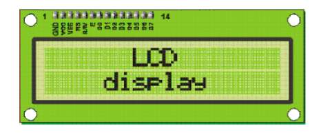
Fig 3.13:LCD display
A model described here is for its low price and great possibilities most frequently used in practice. It is based on the HD44780 microcontroller (Hitachi) and can display messages in two lines with 16 characters each. It displays all the alphabets, Greek letters, punctuation marks, mathematical symbols etc. In addition, it is possible to display symbols that user makes up on its own.
Automatic shifting message on display (shift left and right), appearance of the pointer, backlight etc. are considered as useful characteristics.
3.6.1. Pins Functions:
There are pins along one side of the small printed board used for connection to the microcontroller. There are total of 14 pins marked with numbers (16 in case the background light is built in). Their function is described in the table 3.6:
Table 3.2: Pin functions of LCD
| Pin No | Function | Name |
| 1 | Ground (0V) | Ground |
| 2 | Supply Voltage, 5V(4.7 V-5.3V) | Vcc |
| 3 | Contrast adjustment, through a variable resistor | VEE |
| 4 | Selects command register when low, and the register when high | Register select |
| 5 | Low to write to the register, high to read from the register | Read /Write |
| 6 | Sends data to data pins when a high to low pulse is given | Enable |
| 7 | DB0 | |
| 8 | DB1 | |
| 9 | DB2 | |
| 10 | 8- BIT DATA PINS | DB3 |
| 11 | DB4 | |
| 12 | DB5 | |
| 13 | DB6 | |
| 14 | DB7 | |
| 15 | Backlight Vcc(5V) | Led + |
| 16 | Backlight ground(0V) | Led+ |
3.6.2. LCD screen:
LCD screen shown in figure 3.15 consists of two lines with 16 characters each. Each character consists of 5×7 dot matrix. Contrast on display depends on the power supply voltage and whether messages are displayed in one or two lines. For that reason, variable voltage 0-Vdd is applied on pin marked as Vee. Trimmer potentiometer is usually used for that purpose. Some versions of displays have built in backlight (blue or green diodes). When used during operating, a resistor for current limitation should be used (like with any LE diode).
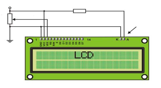
Figure 3.14: LCD connection
Contrast
LCD backlight
330R
5k
3.6.3. LCD Basic Commands:
All data transferred to LCD through outputs D0-D7 will be interpreted as commands or as data, which depends on logic state on pin RS: RS = 1 – Bits D0 – D7 are addresses of characters that should be displayed. Built in processor addresses built in “map of characters” and displays corresponding symbols. Displaying position is determined by DDRAM address. This address is either previously defined or the address of previously transferred character is automatically incremented.
RS = 0 – Bits D0 – D7 are commands which determine display mode. List of commands which LCD recognizes are very important to write the code for LCD. The below table 3.4 shows the LCD commands which are useful in the writing of code to display the data.
Table 3.3: LCD commands table
| Command | RS | RW | D7 | D6 | D5 | D4 | D3 | D2 | D1 | D0 | Execution
Time |
|
| Clear display | 0 | 0 | 0 | 0 | 0 | 0 | 0 | 0 | 0 | 1 | 1.64Ms | |
| Cursor home | 0 | 0 | 0 | 0 | 0 | 0 | 0 | 0 | 1 | x | 1.64mS | |
| Entry mode set | 0 | 0 | 0 | 0 | 0 | 0 | 0 | 1 | I/D | S | 40uS | |
| Display on/off control | 0 | 0 | 0 | 0 | 0 | 0 | 1 | D | U | B | 40uS | |
| Cursor/Display Shift | 0 | 0 | 0 | 0 | 0 | 1 | D/C | R/L | x | x | 40uS | |
| Function set | 0 | 0 | 0 | 0 | 1 | DL | N | F | x | x | 40uS | |
| Set CGRAM address | 0 | 0 | 0 | 1 | CGRAM address | 40uS | ||||||
| Set DDRAM address | 0 | 0 | 1 | DDRAM address | 40uS | |||||||
| Read “BUSY” flag (BF) | 0 | 1 | BF | DDRAM address | – | |||||||
| Write to CGRAM or DDRAM | 1 | 0 | D7 | D6 | D5 | D4 | D3 | D2 | D1 | D0 | 40uS | |
| Read from CGRAM or DDRAM | 1 | 1 | D7 | D6 | D5 | D4 | D3 | D2 | D1 | D0 | 40uS | |
I/D 1 = Increment (by 1) R/L 1 = Shift right
0 = Decrement (by 1) 0 = Shift left
S 1 = Display shift on DL 1 = 8-bit interface
0 = Display shift off 0 = 4-bit interface
D 1 = Display on N 1 = Display in two lines
0 = Display off 0 = Display in one line
U 1 = Cursor on F 1 = Character format 5×10 dots
0 = Cursor off 0 = Character format 5×7 dots
B 1 = Cursor blink on D/C 1 = Display shift
0 = Cursor blink off 0 = Cursor shift
3.6.4. LCD Connection:
Depending on how many lines are used for connection to the microcontroller, there are 8-bit and 4-bit LCD modes. The appropriate mode is determined at the beginning of the process in a phase called “initialization”. In the first case, the data are transferred through outputs D0-D7 as it has been already explained. In case of 4-bit LED mode, for the sake of saving valuable I/O pins of the microcontroller, there are only 4 higher bits (D4-D7) used for communication, while other may be left unconnected.
Consequently, each data is sent to LCD in two steps: four higher bits are sent first (that normally would be sent through lines D4-D7), four lower bits are sent afterwards. With the help of initialization, LCD will correctly connect and interpret each data received. Besides, with regards to the fact that data are rarely read from LCD (data mainly are transferred from microcontroller to LCD) one more I/O pin may be saved by simple connecting R/W pin to the Ground. Such saving has its price. Even though message displaying will be normally performed, it will not be possible to read from busy flag since it is not possible to read from display.
3.6.5. LCD Initialization:
Once the power supply is turned on, LCD is automatically cleared. This process lasts for approximately 15mS. After that, display is ready to operate. The mode of operating is set by default. This means that:
1. Display is cleared
2. Mode
DL = 1 Communication through 8-bit interface
N = 0 Messages are displayed in one line
F = 0 Character font 5 x 8 dots
3. Display/Cursor on/off
D = 0 Display off
U = 0 Cursor off
B = 0 Cursor blink off
3. Character entry
ID = 1 Addresses on display are automatically incremented by 1
S = 0 Display shift off
Automatic reset is mainly performed without any problems. If for any reason power supply voltage does not reach full value in the course of 10mS, display will start perform completely unpredictably.
If voltage supply unit cannot meet this condition or if it is needed to provide completely safe operating, the process of initialization by which a new reset enabling display to operate normally must be applied.
Algorithm according to the initialization is being performed depends on whether connection to the microcontroller is through 4- or 8-bit interface. All left over to be done after that is to give basic commands and of course- to display messages.
3.6.6. Contrast control:
To have a clear view of the characters on the LCD, contrast should be adjusted. To adjust the contrast, the voltage should be varied. For this, a preset is used which can behave like a variable voltage device. As the voltage of this preset is varied, the contrast of the LCD can be adjusted.


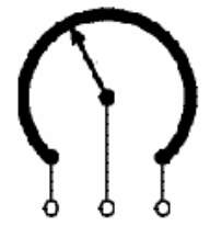
Wiper
Track
Terminals
Figure 3.15: Variable resistor
3.6.7. Potentiometer:
Variable resistors shown in figure 3.16 used as potentiometers have all three terminals connected. This arrangement is normally used to vary voltage, for example to set the switching point of a circuit with a sensor, or control the volume (loudness) in an amplifier circuit. If the terminals at the ends of the track are connected across the power supply, then the wiper terminal will provide a voltage which can be varied from zero up to the maximum of the supply. The symbol of potentiometer is shown in figure 3.17.
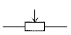
Figure 3.16: Potentiometer symbol
3.6.8. Presets:
These are miniature versions of the standard variable resistor. They are designed to be mounted directly onto the circuit board and adjusted only when the circuit is built. For example, to set the frequency of an alarm tone or the sensitivity of a light-sensitive circuit, a small screwdriver or similar tool is required to adjust presets.
Presets are much cheaper than standard variable resistors so they are sometimes used in projects where a standard variable resistor would normally be used. Preset symbol is shown in figure 3.18. Multiturn presets are used where very precise adjustments must be made. The screw must be turned many times (10+) to move the slider from one end of the track to the other, giving very fine control.

Figure 3.17: Preset symbol
3.7. GSM Module:
The short message system (SMS) of a standard mobile phone can be used for much more than just exchanging cryptic message. This application finds a humble mobile working for controlling external equipments. The SMS service provides by the service providers are comparatively low cost. Hence the system is highly efficient and low-cost.
Mobile phones have become a widespread means of communication. It becomes a part of everyday life with ever more people enjoying the service and extra freedom they provide. It works on the basis of Global System for Mobile Communication (GSM). A subscriber from any systems can access telecommunication services by using a Subscriber Identify Module (SIM) card in a handset suitable for the network on the visited system The Short Message Service allows text messages to be sent and received to and from mobile telephones. The text can comprise words or numbers or an alphanumeric combination. Because Simple person – to – person messaging is such an important component of total SMS traffic volumes, anything that simplifies message generation as well as extended utility of the SMS being sent is an important enabler of Short Message Service.
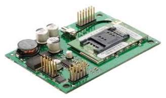
Figure 3.18:GSM Module
The main aim of this project is to control the car engine. We will connect Hardware kit to car engine. The hardware kit consists of microcontroller and GSM modem
A GSM modem is a specialized type of modem which accepts a SIM card, and operates over a subscription to a mobile operator, just like a mobile phone. From the mobile operator perspective, a GSM modem looks just like a mobile phone.
When a GSM modem is connected to a computer, this allows the computer to use the GSM modem to communicate over the mobile network. While these GSM modems are most frequently used to provide mobile internet connectivity, many of them can also be used for sending and receiving SMS and MMS messages.
Now SMS Light can send and receive SMS and MMS Messages using a GSM modem:
A GSM modem can be a dedicated modem device with a serial, USB or Bluetooth connection, or it can be a mobile phone that provides GSM modem capabilities.
For the purpose of this document, the term GSM modem is used as a generic term to refer to any modem that supports one or more of the protocols in the GSM evolutionary family, including the 2.5G technologies GPRS and EDGE, as well as the 3G technologies WCDMA, UMTS, HSDPA and HSUPA.
A GSM modem exposes an interface that allows applications such as Now SMS to send and receive messages over the modem interface. The mobile operator charges for this message sending and receiving as if it was performed directly on a mobile phone. To perform these tasks, a GSM modem must support an “extended AT command set” for sending/receiving SMS messages, as defined in the ETSI GSM 07.05 and 3GPP TS 27.005 specifications.
GSM modems can be a quick and efficient way to get started with SMS, because a special subscription to an SMS service provider is not required. In most parts of the world, GSM modems are a cost effective solution for receiving SMS messages, because the sender is paying for the message delivery.
A GSM modem can be a dedicated modem device with a serial, USB or Bluetooth connection, such as the Falcon Samba 75. (Other manufacturers of dedicated GSM modem devices include Wavecom, Multitech and iTegno. We’ve also reviewed a number of modems on our technical support blog.) To begin, insert a GSM SIM card into the modem and connect it to an available USB port on your computer.
A GSM modem could also be a standard GSM mobile phone with the appropriate cable and software driver to connect to a serial port or USB port on your computer. Any phone that supports the “extended AT command set” for sending/receiving SMS messages, as defined in ETSI GSM 07.05 and/or 3GPP TS 27.005, can be supported by the Now SMS & MMS Gateway. Note that not all mobile phones support this modem interface.
Due to some compatibility issues that can exist with mobile phones, using a dedicated GSM modem is usually preferable to a GSM mobile phone. This is more of an issue with MMS messaging, where if you wish to be able to receive inbound MMS messages with the gateway, the modem interface on most GSM phones will only allow you to send MMS messages. This is because the mobile phone automatically processes received MMS message notifications without forwarding them via the modem interface. It should also be noted that not all phones support the modem interface for sending and receiving SMS messages. In particular, most smart phones, including Blackberries, iPhone, and Windows Mobile devices, do not support this GSM modem interface for sending and receiving SMS messages at all at all. Additionally, Nokia phones that use the S60 (Series 60) interface, which is Symbian based, only support sending SMS messages via the modem interface, and do not support receiving SMS via the modem interface.
The Future of GSM:
GSM together with other technologies is part of an evolution of wireless mobile telecommunication that includes High-Speed Circuit-Switched Data (HSCSD), General Packet Radio System (GPRS), Enhanced Data rate for GSM Evolution (EDGE), and Universal Mobile Telecommunications Service (UMTS).
GSM Network Operators:
T-Mobile and Cingular operate GSM networks in the United States on the 1,900 MHz band. GSM networks in other countries operate at 900, 1,800, or 1,900 MHz.
GSM (Global System for Mobile Communications):
Originally from Group Special Mobile is the most popular standard for mobile telephony systems in the world. The GSM Association, its promoting industry trade organization of mobile phone carriers and manufacturers, estimates that 80% of the global mobile market uses the standard.[1] GSM is used by over 1.5 billion people[2] across more than 212 countries and territories.[3] This ubiquity means that subscribers can use their phones throughout the world, enabled by international roaming arrangements between mobile network operators. GSM differs from its predecessor technologies in that both signaling and speech channels are digital, and thus GSM is considered a second generation (2G) mobile phone system. This also facilitates the wide-spread implementation of data communication applications into the system.
The GSM standard has been an advantage to both consumers, who may benefit from the ability to roam and switch carriers without replacing phones, and also to network operators, who can choose equipment from many GSM equipment vendors.[4] GSM also pioneered low-cost implementation of the short message service (SMS), also called text messaging, which has since been supported on other mobile phone standards as well. The standard includes a worldwide emergency telephone number feature (112).[5]
Newer versions of the standard were backward-compatible with the original GSM system. For example, Release ’97 of the standard added packet data capabilities by means of General Packet Radio Service (GPRS). Release ’99 introduced higher speed data transmission using Enhanced Data Rates for GSM Evolution (EDGE).
GSM carrier frequencies:
GSM networks operate in a number of different carrier frequency ranges (separated into GSM frequency ranges for 2G and UMTS frequency bands for 3G), with most 2G GSM networks operating in the 900 MHz or 1800 MHz bands. Where these bands were already allocated, the 850 MHz and 1900 MHz bands were used instead (for example in Canada and the United States). In rare cases the 400 and 450 MHz frequency bands are assigned in some countries because they were previously used for first-generation systems.
Most 3G networks in Europe operate in the 2100 MHz frequency band.
Regardless of the frequency selected by an operator, it is divided into timeslots for individual phones to use. This allows eight full-rate or sixteen half-rate speech channels per radio frequency. These eight radio timeslots (or eight burst periods) are grouped into a TDMA frame. Half rate channels use alternate frames in the same timeslot. The channel data rate for all 8 channels is 270.833 Kbit/s, and the frame duration is 4.615 ms.
The transmission power in the handset is limited to a maximum of 2 watts in GSM850/900 and 1 watt in GSM1800/1900.
Check if your GSM phone or modem supports SMS text mode:
To check if your modem supports this text mode, you can try the following command:
AT+CMGF=1
If the modem responds with “OK” this mode is supported. Please note that using this mode it is only possible to send simple text messages. It is not possible to send multipart, Unicode, data and other types of messages.
Setting up the modem
If the modem contains a SIM card with is secured with a PIN code, we have to enter this pin code first:
AT+CPIN=”0000″
Please not that in most cases you have only 3 attempts to set the correct PIN code. After setting the PIN code, wait some seconds before issuing the next command to give the modem some time to register with the GSM network.
In order to send a SMS, the modem has to be put in SMS text mode first using the following command:
AT+CMGF=1
In text mode there are some additional parameters that can be set. Using the following command we can read the current values:
AT+CSMP?
The modem wills response with a string like this:
+CSMP: 1, 169, 0,0OK
The first value is a combination of some option bits:
| bit 7 | RP | Reply path, not used in text mode |
| bit 6 | UDHI | User Data Header Information |
| bit 5 | SRR | Set this bit to request a delivery report |
| bit 3,4 | VPF | Validity Period, set b4=1 if a VP value is present |
| bit 2 | RD | Reject Duplicates, do not return a message ID when a message with the same destination and ID is still pending |
| bit 0,1 | MTI | Message Type Indicatorb1=0 & b0=0 -> SMS-DELIVERb1=0 & b0=1 -> SMS-SUBMIT |
Bit 0 of the message is always set when sending messages (SMS-SUBMIT). So the first value should be 1 or higher. The second parameter sets the Validity Period of the message. This value is encoded as follows:
| 0 – 143 | (VP + 1) x 5 minutes |
| 144 – 167 | 12 Hours + ((VP-143) x 30 minutes) |
| 168 – 196 | (VP-166) x 1 day |
| 197 – 255 | (VP-192) x 1 week |
The third parameter contains the PID (Protocol Identifier). This parameter is only used for advanced messaging. The fourth parameter contains the DCS (Data Coding Scheme). This parameter is used to select the character set/message type. When setting the DCS parameter to ‘0’ standard 7 bit text is send. When setting this parameter to ’16’ the message is sent as a flash message.
To send a message with a validity period of 1 day, the parameters have to be set like this:
Bit 0 and 4 of the first field has to be set, so the first value will become 1 + 16 = 17.
Send the following command to the modem to set this parameters:
AT+CSMP=17, 167,0,16
If the modem responds with “OK” ,the modem is ready to send (flash) text messages with a validity period of 1 day.
Sending the message
To send the SMS message, type the following command:
AT+CMGS=”+31638740161″
Replace the above phone number with your own cell phone number. The modem will respond with:
>
You can now type the message text and send the message using the
Hello World!
After some seconds the modem will respond with the message ID of the message, indicating that the message was sent correctly:
+CMGS: 62
The message will arrive on the mobile phone shortly.
Sending an Unicode SMS message
Some modems also have the capability to send Unicode or UCS2 messages without encoding a PDU. You can send Unicode messages by only converting the Unicode data to a HEX string and send this string to the modem.
To check whether your modem supports this mode, just type the following command:
AT+CSCS=?
This command displays the codepages supported by the modem. The modem will respond like this:
+CSCS: (“GSM”,”PCCP437″,”CUSTOM”,”HEX”)
If this string contains “HEX” or “UCS2”, Unicode seems to be supported. To specify that you will use an HEX string to send the message, set the codepage to “HEX” or “UCS2” depending on the modem response. In our example we will set the modem to “HEX”:
AT+CSCS=”HEX”
Next, we have to specify the correct DCS (Data Coding Scheme) for Unicode messages, which is 0x08. We can set this value by changing the fourth parameter of the AT+CSMP command to ‘8’:
AT+CSMP=1,167,0,8
The modem is now ready to send messages as Unicode. Now is the time to send the actual message:
AT+CMGS=”+31638740161″
Replace the above phone number with your own cell phone number. The modem will respond with:
>
The only thing you have to program by yourself, is a simple routine which converts the Unicode string to an hexadecimal string like this:
مرحبا
Which is ‘Hello’ in Arabic will be converted like this:
“06450631062D06280627”
You can send this hexadecimal string to the modem:
06450631062D06280627
After some seconds the modem will respond with the message ID of the message, indicating that the message was sent correctly:
+CMGS: 63
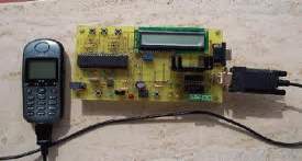
Figure 3.19:GSM module connection to phone
The message will arrive on the mobile phone shortly.
CHAPTER 4: FIRMWARE IMPLEMENTATION OF THE PROJECT DESIGN
This chapter briefly explains about the firmware implementation of the project
4.1.SOURCE CODE:
- Click on the Keil uVision Icon on Desktop
- The following fig will appear
- Click on the Project menu from the title bar
- Then Click on New Project
- Save the Project by typing suitable project name with no extension in u r own folder sited in either C: or D:
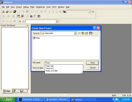
- Then Click on Save button above.
- Select the component for u r project. i.e. Atmel……
- Click on the + Symbol beside of Atmel
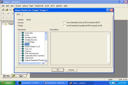
- Select AT89C51 as shown below
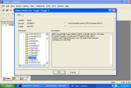
- Then Click on “OK”
- The Following fig will appear
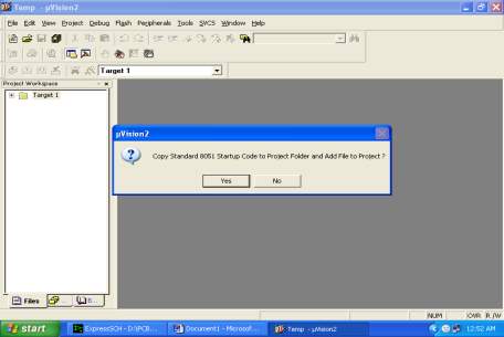
- Then Click either YES or NO………mostly “NO”
- Now your project is ready to USE
- Now double click on the Target1, you would get another option “Source group 1” as shown in next page.
- Click on the file option from menu bar and select “new”
- The next screen will be as shown in next page, and just maximize it by double clicking on its blue boarder.
- Now start writing program in either in “C” or “ASM”
- For a program written in Assembly, then save it with extension “. asm&rdquo and for “C” based program save it with extension “ .C”
- Now right click on Source group 1 and click on “Add files to Group Source”
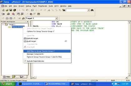
- Now you will get another window, on which by default “C” files will appear.
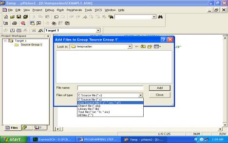
- Now select as per your file extension given while saving the file
- Click only one time on option “ADD”
- Now Press function key F7 to compile. Any error will appear if so happen.
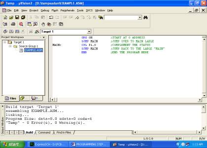
- If the file contains no error, then press Control+F5 simultaneously.
- The new window is as follows
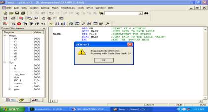
- Then Click “OK”
- Now Click on the Peripherals from menu bar, and check your required port as shown in fig below
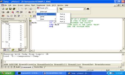
- Drag the port a side and click in the program file.
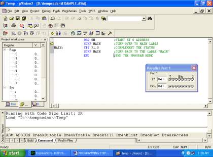
- Now keep Pressing function key “F11” slowly and observe.
- You are running your program successfully
4.2. Proload:
Proload is software which accepts only hex files. Once the machine code is converted into hex code, that hex code has to be dumped into the microcontroller and this is done by the Proload. Proload is a programmer which itself contains a microcontroller in it other than the one which is to be programmed. This microcontroller has a program in it written in such a way that it accepts the hex file from the Keil compiler and dumps this hex file into the microcontroller which is to be programmed. As the Proload programmer kit requires power supply to be operated, this power supply is given from the power supply circuit designed above. It should be noted that this programmer kit contains a power supply section in the board itself but in order to switch on that power supply, a source is required. Thus this is accomplished from the power supply board with an output of 12volts.
Features:
- Supports major Atmel 89 series devices
- Auto Identify connected hardware and devices
- Error checking and verification in-built
- Lock of programs in chip supported to prevent program copying
- 20 and 40 pin ZIF socket on-board
- Auto Erase before writing and Auto Verify after writing
- Informative status bar and access to latest programmed file
- Simple and Easy to use
- Works on 57600 speed
Description:
It is simple to use and low cost, yet powerful flash microcontroller programmer for the Atmel 89 series. It will Program, Read and Verify Code Data, Write Lock Bits, Erase and Blank Check. All fuse and lock bits are programmable. This programmer has intelligent onboard firmware and connects to the serial port. It can be used with any type of computer and requires no special hardware. All that is needed is a serial communication ports which all computers have.
All devices have signature bytes that the programmer reads to automatically identify the chip. No need to select the device type, just plug it in and go! All devices also have a number of lock bits to provide various levels of software and programming protection. These lock bits are fully programmable using this programmer. Lock bits are useful to protect the program to be read back from microcontroller only allowing erase to reprogram the microcontroller. The programmer connects to a host computer using a standard RS232 serial port. All the programming ‘intelligence’ is built into the programmer so you do not need any special hardware to run it. Programmer comes with window based software for easy programming of the devices.
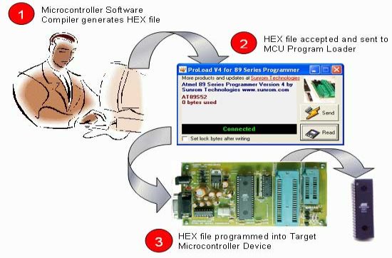
Programming Software:
Computer side software called ‘Proload V4.1’ is executed that accepts the Intel HEX format file generated from compiler to be sent to target microcontroller. It auto detects the hardware connected to the serial port. It also auto detects the chip inserted and bytes used. Software is developed in Delphi 7 and requires no overhead of any external DLL.
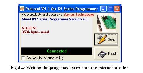
CHAPTER 5: RESULTS AND DISCUSSIONS
5.1 RESULTS:
The Electronic Distribution Of Goods In Ration Shop is based on GSM and RFID Technology which is used for Ration materials distribution in ration shops. Initially everyone will be provided an RFID Card, instead of a ration card. If the customer needs to get any ration material, the user has to show the ration RFID tag card to the RFID reader , the reader will recognize the RFID numbers show by the user. Each user will have a unique number, which is not visible to the user. This recognized RFID number will be given to a microcontroller, which compared the input number with the database. Before starting the system, the unique RFID number of the ration user will be programmed in the controller, such as User name and password., so that the controller will recognize the data coming from RFID by comparing with the database. Once the user is identified, the ration items to be dispensed will be displayed on the LCD screen, the user has to feed the comments such as the weight he is going to buy. As the dispensing process is going on simultaneously the controller will send a command to GSM Modem, to send the text SMS to the user and authorities about the ration item, he or she purchased
Working Procedure:
5.2 ADVANTAGES
1.cost effective approach
2.This system is very effective ,accurate,simple and power conservative.
3.time effective approach
4.This system helps to maintain data correctly.
CONCLUSION AND FUTURE SCOPE
CONCLUSION
In ration shop several drawbacks are there like material robbery, corruption, malpractices, long waiting time to collect materials, low processing speed. To overcome above problems the mechanized rationing scheme is needed. Here the automatic ration shop concerned smart card and controller for distributing the materials. At this time ration card is changed by smart card and send the stock details to government head office using GSM module. Here all the works are done automatically without any manpower. So this proposed system used to avoid the corruption, goods theft, forgery and also they reduce the user’s waiting time. This system also suggested maintaining the stock details properly and updating the details easily. They provide a secure, safe and efficient way of fair price shops.
FUTURE SCOPE
In future we can improve the memory and can store the data of all customers.If the groceries are not upto the necessity, information can be sent to both government authorities and the card holders using gsm technology.we can authenticate the rfid cards with passwords.we can improve the customer satisfaction by improving the security.
REFERENCES
[1] www.schneiderelectric.com.hk/resources/access/text/rfidreader
[2] http://archive.computerhistory.org/resources/access Oral History Panel, retrieved 2011 June 28 page 4
[3] Microchip unveils PIC16C84, a reprogrammable EEPROM-based 8-bit microcontroller 1993
[4] 8051 microcontrollers: an applications-based introduction
[5] BBC, (2003), Supermarket Tries Out Smart Tagging, BBC News, www.bbc.co.uk, 16 January.
[6] www.schneiderelectric.com.hk/…/Sympholux_Shopping_Mall
[7] RFID JOURNAL, 2002-2007, REFFERD 6.8.2007, http://www.rfidjournal.com
[8] http://www.vbtutor.net/vb6/vbtutor.html visual basic 6 tutorial
Cite This Work
To export a reference to this article please select a referencing stye below:
Related Services
View all


Related Content
All TagsContent relating to: "Technology"
Technology can be described as the use of scientific and advanced knowledge to meet the requirements of humans. Technology is continuously developing, and is used in almost all aspects of life.
Related Articles

DMCA / Removal Request
If you are the original writer of this dissertation and no longer wish to have your work published on the UKDiss.com website then please: