Silicon Carbide (SiC) Based Devices
Info: 7824 words (31 pages) Dissertation
Published: 16th Dec 2019
Tagged: TechnologyElectronics
- Introduction
In power semiconductor industry, Silicon Carbide (SiC) based devices become a prominent alternative in compared to Silicon (Si) based device due to its superior characteristics. For example, in the term of power dissipation; high voltage blocking capability due to high breakdown electrical field- 4×10⁶V/cm, high electron drift velocity – 2×107cm/s, high thermal conductivity – 4.9W/cm-°K, large bandgap energy leads to higher temperature operation capability, higher radiation hardness, and relatively higher thermal conductivity. Recently, the mobile communication systems have seen a fast development in which high-frequency power transistors are required by the base stations. In fact, in the satellite communication and Military Radar field; traveling wave tube and magnetrons are been replace by high-power transistors due to a compact size, low weight, and long life of the transistor. Thus, silicon carbide (SiC) device becomes more attracting in the market.
Silicon carbide (SiC) devices can work under such an outrageous condition that it is required to empower critical upgrades to a far-extending assortment of applications and systems. Silicon carbide (SiC) devices are used in high-temperature, high-power, and highly radiated condition. These devices improve the high voltage switching for efficient power distribution, to drive powerful microwave electronics for military radar and communication, and controls the fuel or engine of aircraft and automobile for higher efficiency. In compared to the silicon carbide (SiC) devices, the other semiconductors are not able to perform under extreme condition [1-2].
In addition, the reverse recovery time is the effect of recombination and sweep out of holes and electrons. The reverse recovery time of silicon carbide (SiC) device totally depends on the internal device parameters and the external operating conditions. The internal parameters are related to a manufacturing process. But the external parameters are the turn-off voltage, forward current, commuting di/dt, and junction temperature. This parameter is used to analyze the performance of the silicon carbide (SiC) devices. At high junction temperature, the turn-off voltage performance of the Silicon carbide (SiC) devices get worse but in compared to silicon (Si) devices, it’s much better. Silicon carbide (SiC) devices can work at high temperature at 200oC. The feature of Silicon carbide (SiC) devices like wide bandgap energy, high thermal conductivity, and high dielectric breakdown which improve the reverse recovery time.
The Silicon Carbide (SiC) devices have specific on-resistance (Ron). The on-resistance (Ron) of the device rise when current flows through parasitic body diodes for mass production. Due to the parasitic body diodes, the base planes are dislocated, induce expansion of stacking faults in 4H-SiC epilayers. The on-resistance (Ron) and drain to source resistance of silicon carbide (SiC) devices have the effects like self-heating, channel length modulation and temperature effects on the parameters as mobility. The main reason behind the on-resistance (Ron) is not only the active area of the silicon power die. But the bonding wire configuration and top metallization debiasing effects have equal importance. Two of the conventional MESFET device are compared. The constant current from the drain to source is 8Amp. The die size is 13.2mm2 and the active area is 10mm2. The blocking voltage is 1200Volt. The typical on-resistance (Ron) is 0.09
n = integer = 1 for the existing ground state.
This type of inconsistency happens between the actual binding energy (59 meV) and the effective mass. The improved voltage of the central cell is approx. 53 meV. The large central cell correction which have wave function create defects like much more localization. If the number of correction increase than the more localization increase in wave function. In fact, the interaction among the core and central cell is more. This is the main reason that the P0 line is shorter than Q0 line in the spectrum. The electric photoluminescence is not limited to silicon carbide. In silicon carbide (SiC), the ratio of the bound excitons luminescence and the free electrons provide accurate doping level [31].
Since the defects of nitrogen in cubic site is less than the correction of the central cell. In pure crystal, the absorption of the bandgap photons can create hole-electron pairs, and this bandgap photon binds the free excitons. Thus, freely moving in the crystal state is possible until the recombination occur. If similar process for some part of nitrogen is required than there is need to have free excitons. The free excitons of some part of nitrogen will lose the energy and after all this it try to bind with the center that have four-particle known as the bound excitons. This four-particle can form electron-hole pair.
- Properties of Silicon Carbide (SiC).
- Crystal Structure.
In the fourth column of periodic table, there are semiconductors materials. The semiconductors materials are the group of materials that are intermediate of metal and insulators in case of conductivities. This material neither they are good conductor nor they are good insulator. The characteristic of this material varies with change in temperature or by adding impurities. Due to wide variation in characteristic helps the electronic device to perform different function.
In recent year, Silicon carbide (SiC) device has capabilities to replace the silicon (Si) device due to the feature like high voltage blocking capability, high temperature operation capability, and a much lower on-resistance in compare to silicon device. Silicon carbide is a crystalline compound of silicon and carbon, and known by carborundum. Its available rarely in the nature in the form of mineral moissanite. Silicon carbide is non-oxide ceramic with properties like high hardness and strength, high melting point, thermal and chemical stability, oxidation resistance, high erosion resistance.
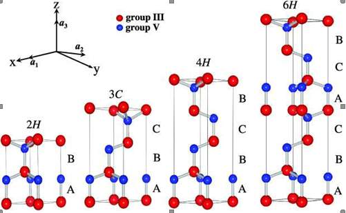
Figure 2.5. The Silicon Carbide (SiC) material structure.
Silicon carbide have more than 200 polytype [40]. Figure 2.5 contains the structure of the silicon carbide. There are three standard structure of silicon carbide 1). Cubic crystal 2). Hexagonal crystal 3). Rhombohedra crystal. The 3C, 4H, 6H and 15R are the common polytype of silicon carbide. The band gap energy of silicon carbide change from 2.3 eV for 3C-SiC to 3.2 eV for 4H-SiC. The silicon carbide hexagonal structures 4H-SiC and 6H-SiC are the polytypes available in bulk wafer. In Silicon carbide, the hexagonal polytypes 6H and 4H have the great capabilities for electronic devices. The main difference among the 6H and 4H is the electron mobility of 6H-SiC is half of the 4H-SiC which is perpendicular to c-axis, and 4H-SiC is 10 times of the that of 6H-SiC parallel to the c-axis [28].
- 3C-SiC.
One of biggest advantage of the 3C-SiC is that it can be grown on the silicon substrate but it is cheaper quality. In future, the combine integration of 3C-SiC device and the silicon device can be done on the same chip. In compare to 4H-SiC device, the 3C-SiC device has more electrons mobility and less hole mobility. Among all the polytype devices, the 3C-SiC has main drawback that it has low bandgap and low breakdown voltage. Figure 2.6 shows about the structure of the 3C-SiC device. The 3C-SiC beta version is use for the commercial. Presently, the used of the beta form is more as heterogeneous catalysts in compare to the alpha form.
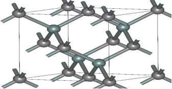
Figure 2.6. The Structure of (β) 3C-SiC.
- 4H-SiC.
A small anisotropy in which the low field mobility of silicon device is double the 4H-SiC device. The mobility is 20% higher in the parallel direction to c-axis. The anisotropy of the 4H-SiC rest on the electric field, and in the c-axis direction the saturation velocity is 20 % due to high electric field. The 4H-SiC is the mature polytypes which is systematically characterized. At present, the polytype 4H-SiC having good transport properties due this its more favorable in commercial products. Figure 2.7 display the 4H-SiC crystal structure.
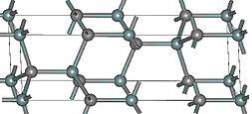
Figure 2.7. The Structure of 4H-SiC.
- 6H-SiC.
In 6H-SiC crystallographic lattice, the long repetition cause the large anisotropy. The mobility in 6H-SiC 25% in the perpendicular direction to the c-axis, and in parallel direction 7% respectively in compare Silicon (Si). Moreover, in 6H-SiC the saturation velocity is 0.2107 cm/s in perpendicular direction to the c-axis and 0.6107 cm/s in parallel direction. The figure 2.8 shows 6H-SiC crystal structure.
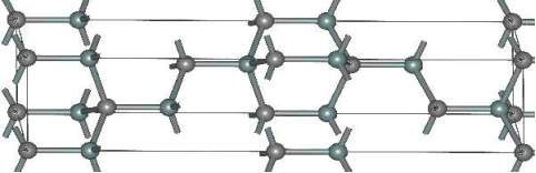
Figure 2.8. The Structure of 6H-SiC.
- Characteristics of Silicon Carbide (SiC).
In all the semiconductors, in compare silicon carbide (SiC) has more wide band gap. This means it’s not temperature sensitive. The advantage of the wide band gap is tolerance to high-temperature, more speed due to high-frequency and high-power due good I-V characteristic.
The fundamental properties of silicon carbide (SiC) polytypes and the silicon (Si) semiconductor is given in Table 1. In Table 2 display about the semiconductor material properties.
| Quantity | 3C-SiC | 4H-SiC | 6H-SiC | Silicon |
| Thermal conductivity
(W/cm-1K-1) at 300K(cm-3) |
3.2 | 3.7 | 4.9 | 1.5 |
| Intrinsic carrier concentration
at 300K (cm-3) |
1.5×10⁻¹ | 5×10⁻⁹ | 1.6×10⁻⁶ | 1.0×10²⁰ |
| Saturation velocity (cm s-1)
parallel to c-axis |
— | 2.0×10⁷ | 2.0×10⁷ | 1.0×10⁷ |
| Electronic mobility (cm2v-1s-1) | 800 | 1000 | 400 | 1400 |
| Hole mobility (cm2v-1s-1) | 40 | 115 | 101 | 471 |
Table 2.1. The Silicon Carbide (SiC) polytypes and silicon (Si) material properties[43].
| Properties | Si | GaAs | 3C-SiC | 6H-SiC | 4H-SiC |
| Band gap (eV)
(T<5K) |
1.12 | 1.43 | 2.40 | 3.02 | 3.26 |
| Saturated electron drift velocity
(107 cm s-1) |
1.0 | 2.0 | 2.5 | 2.0 | 2.0 |
| Breakdown voltage field
(MV cm-1) |
0.25 | 0.3 | 2.12 | 2.5 | 2.2 |
| Thermal conductivity
(W cm-1 K-1) |
1.5 | 0.5 | 3.2 | 4.9 | 3.7 |
| Dielectric constant | 11.8 | 12.8 | 9.7 | 9.7 | 9.7 |
| Physical stability | Good | Fair | Excellent | Excellent | Excellent |
Table 2.2. Comparison of several important semiconductor material properties[44].
The thermal conductivity of the silicon carbide is above 1.5 W/cm-1K-1 as displayed in table 2.1 respectively. The thermal conductivity of silicon carbide is much better than metal conductors. Thus, the dissipation of the heat is quicker. Moreover, silicon carbide (SiC) is resistant to chemical exposer, and highly resilient to radiation. Silicon carbide has high electric field intensity in compare to silicon its 10 times respectively, and saturation electron drift velocity is higher than GaAs.
- Energy Band Diagram.
The energy combination of molecular orbital in a graphical image display the energy bands. There is mass amount of molecular energies which result in formation different energy bands [57]. The figure 2.9 is the energy band diagram shows the various molecular energies.
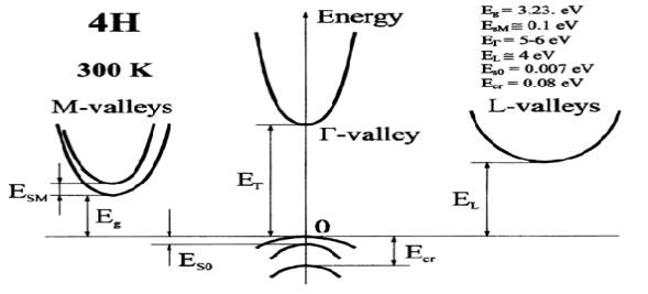
Fig. 2.9. The Silicon Carbide (SiC), 4H Band structure. Important minima of the conduction band and maxima of the valence band. 300K.
Eg = 3.23 eV = Energy Gap.
ET = 5-6.0 eV = Energy at T Valleys.
EL ~= 4.0 eV = Energy at L Valleys.
EsM ~= 0.1 eV = Energy at M Valleys.
Ecr = 0.08 eV = Energy of crystal field splitting in valence band.
Eso = 0.007 eV = Energy of spin-orbital splitting in valence band.
In the figure 2.9 shows the energy band diagram of 4H-SiC. In L-valley the conduction band minima and valence band maxima at k ≠ 0 where the energy band gap of 4H-SiC is 3.24eV respectively. Therefore, the semiconductor is available in the indirect bandgap. The energy bandgap in T valley varies from (ET)5 eV to 6 eV, and the energy bandgap in L valley is EL = 4 eV. The split off band in the valence band is 0.007 eV. The bandgap which is temperature dependent can be calculated from the equation (1).
The energy band gap of 3.23eV of 4H-SiC is found in the L-valley at the conduction band minima and valence band maxima at k ≠ 0 and therefore, semiconductor is found to be indirect bandgap. The bandgap energy in τ valley differs from 5-6 eV and the bandgap energy gap in L valley is (EL) is 4 eV. The split off band in the valence band is 0.007 eV. The separation energy between low and upper conduction bands in M-valleys. The temperature dependent band gap can be calculated from the following Equation (1).
Eg = Eg
(0)-6.5×10⁻⁴x
T2(T+1300)
……………………………………………………………………………(1).
Where,
Eg = Indirect Band-gap indirect of 4H-SiC.
T = Temperature (300 K)
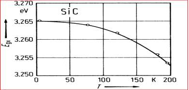
Figure 2.10. The 4H-SiC Excitonic Energy vs. Temperature.
In Figure 2.10 it displays the graph of temperature versus the excitonic energy gap of SiC, and in Figure 2.11 displays the energy band diagram for 3C, 4H and 6H SiC materials at different temperatures.
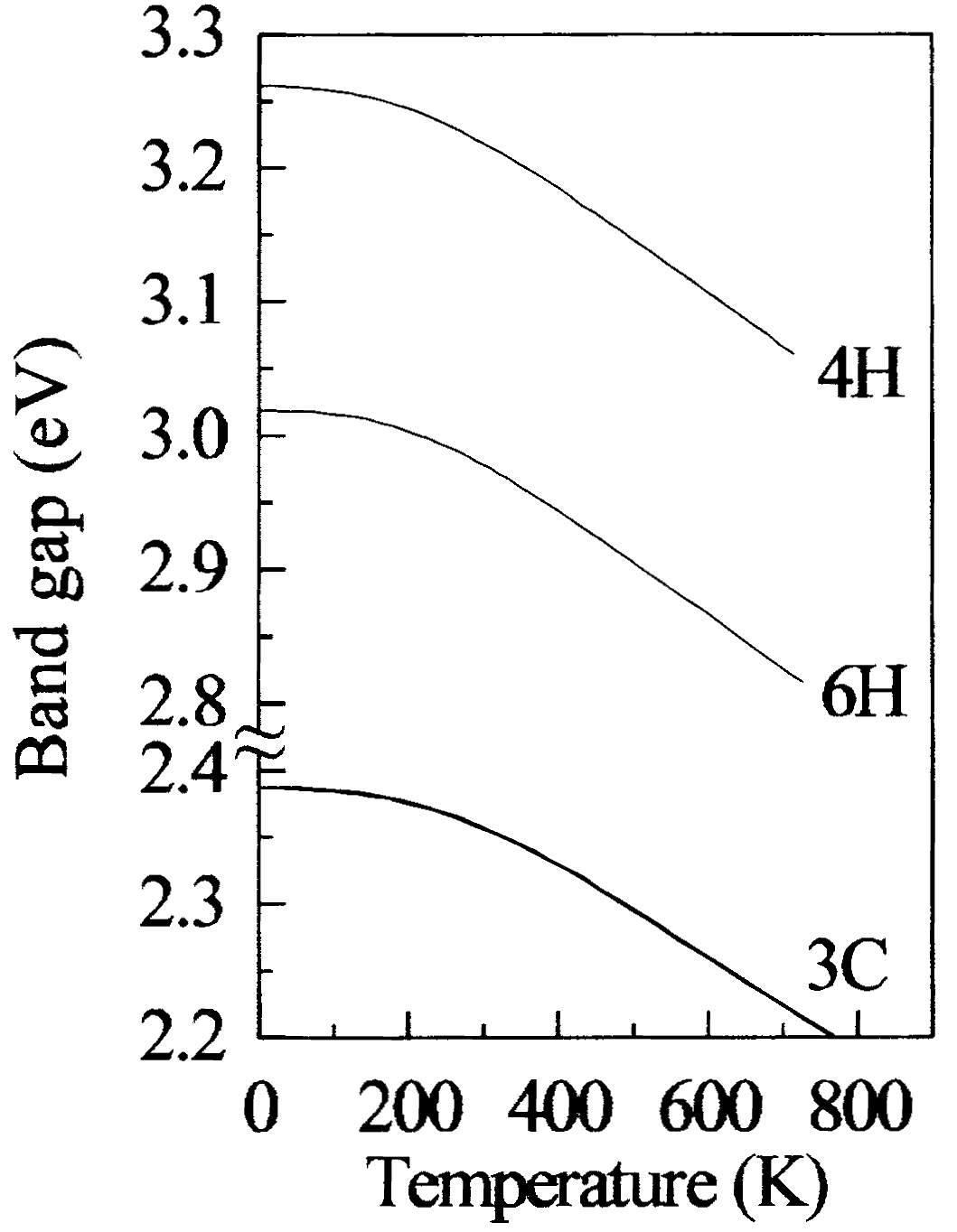
Figure 2.11. The Band gap for 3C, 4H and 6H Silicon Carbide (SiC).
As it can be seen from the figure 2.11, at temperature 700oK the bandgap energy of 6H-SiC differs from 2.8 eV to 3.03 eV respectively, and the bandgap energy of 3C-SiC differs from 2.2 eV to 2.38 eV respectively. To obtain good wide bandgap for silicon carbide (SiC), intrinsic carrier concentration is main parameter to take in consideration. The intrinsic concentration can be calculated through equation (2).
ni =NC. NV.12.exp-Eg2kBT
……………………………………………………………………………………(2).
Where,
NC
= effective density of states in the conduction band (
NC
) and
T = Temperature in K
The effective density of states in the conduction band (NC) can be derived by Equation 3.
Nc= 3.25 x 10¹⁴ x
T32
(cm-3) …………………………………………………………………………..…. (3).
The effective density of states in the valence band (NV) can be derived by Equation 4.
NV= 4.8×10¹⁵ x
T32
(cm-3)………………………………………………………………..……………… (4).
The Figure 3.12 shows the temperature dependence intrinsic concentration of 3C, 4H and 6H SiC calculated from the Equation (3) and (4).
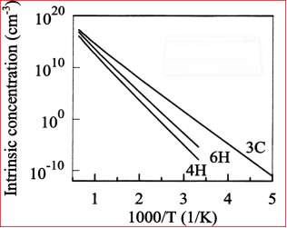
Figure 2.12. The Intrinsic carrier concentration of 3C, 4H and 6H Silicon Carbide (SiC).
- Drift Velocity Graph for Silicon Carbide (SiC).
In the figure 2.13, the graphs present about the drift velocity vs electric field of the 4H-SiC. There is no negative differential resistance is seen in the graph.
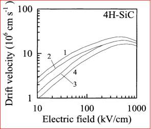
Figure 2.13. Drift Velocity vs. Electric field for 4H-SiC.
The graph describes the curve 1 and 2 to display the drift velocity at 300oK respectively, and the curve 3 and 4 display the drift velocity at 600 oK respectively. It is clear from graph that the drift velocity rises if the electric field till the 800 kV/cm respectively. If the electric field cross over the value 800 kV/cm, then the drift velocity slightly drops. At high electrical field, the drift velocity slightly drops due to the defects in the material. The maturity of silicon carbide (SiC) material growth and characterization is not achieved.
- Fabrication of Silicon Carbide (SiC) MESFET devices.
SiC MESFET and Si FETs have similar fabrication technique. The fabrication process for the SiC is very hard in compare to Si, GaAs and InP, and just few individuals know the fabrication technique in industry. The procedures utilized right now for SiC are youthful. The RF device made of SiC still needs considerably more innovative work to contend financially with Si.
The processes steps clarified here could conceivably be utilized as a part of a specific trial yet it is indispensable data to depict a wide plan. The fabrication method will be comprehended by the reader and will likewise have the capacity to look at below.
A covalent structure of silicon dioxide having high melting point and high insulating properties. In MESFET before the ion implantation, a Silicon Dioxide(SiO2) barrier layer is deposited above the sources and the drain regions. The relevant two techniques to deposit are Thermal Oxidation and Plasma Vapor deposition respectively. As required by metal layer, by sputtering process, a small layer of Ohmic contact are made of nickel or Indium-Oxide-Tin.
In oxidation step, silicon dioxide is developed on silicon carbide wafer by inserting in high-temperature furnace. By using the sputter system, silicon dioxide atoms are fired on silicon carbide wafer from transparent silica-substrate. The thermal oxidation process for silicon wafer and silicon carbide wafer is same. For illustration, to grow 1000 Å of silicon dioxide on silicon carbide wafer 460 Å of silicon carbide was depleted. There are three stage process for thermal oxidation on SiC wafer.
- The silicon carbide wafer is oxidized, and oxygen atom bond is formed with silicon carbide molecule. A dangling bond is formed between Si atom and CO molecule due to insertion of O2 molecule.
- In the diffusion of carbon monoxide were oxide reacts with O2 and produces CO2.
- At starting stage of the oxidation step, near the surface of the silicon carbide substrate, silicon dioxide is formed.
The Chemical formula of the Silicon Dioxide formation [71].
- Silicon Carbide + Oxide Carbon Monoxide + Silicon.
- Carbon Monoxide +Oxygen Carbon Dioxide.
- Silicon +2 x Oxygen Silicon Dioxide.
In sputter system, the ions of the element are vaporized physical to form a thin layer on the target surface. In the chamber, the ions of the element can be fired from the sputter gun towards the selected target. The chamber is maintained at every low-pressure. With the help of RF magnetron, the plasma is forced towards the target. The range of the plasma energy from 4 eV to 20 eV helps the sources material to loosen the atoms of the element due to the molecular-bond of the target. This procedure is called sputtering.
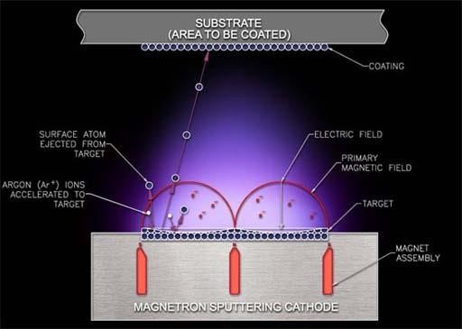
Fig 3.1. The Sputter System.
Argon gas is highly unreactive in nature is most commonly used in the sputtering process. Due to its 8 valance electrons, and strong bonding with other elements makes it more stable. For the sputtering, the plasma is produce from an ideal argon gas, and the ideal gas does not react with any element. Therefore, the argon gas does not react with substrate in the extremely low-pressure chamber. To have chemical reaction in the chamber, with ideal argon gas another gas can be assorted. For example, by mixing 99% of argon and 1% of oxygen, a silicon dioxide coating can be built on the silicon carbide wafer with reduce in the charge interface density. The developing rate of the silicon dioxide is 1000Å/hour.
In an active region of MESFETs, Ion Implantation plays a significant role for the addition of dopants. The N-type device has a P-type insulation substrate. An N-type of epitaxial-layer is full-grown with a N-type conducting channel on the top of P-type substrate. For silicon carbide, Nitrogen or Phosphorous are the N-type dope and boron or aluminum are P-type dope which are entrenched on channel layer. Nickel is deposited on the N+ region for the sources and drain Ohmic contacts.
In case of silicon carbide, it is enormously stable in nature which in return make diffusion step difficult. Therefore, ions are forced to dope through ion-implant method. In which the ions are regulated and vast variety of ions can be used in compared to diffusion procedure.
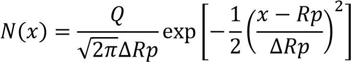
In the host grid atoms, the atoms are blocked on account of the electronic and atomic ceasing system which is in charge of inelastic impact and flexible crash [77]. The electronic and nuclear stopping mechanism obstruct the crystal atom due to the host grid atoms, and in outcome responsible for collision. The dope entering the crystal built impurity. The peak concentration (Np) showing up at the focal point of the bend where x = Rp. The trail (ΔRp) is indicated by standard deviation (σp). A Cross-sectional perspective of the silicon carbide MESFETs is appeared underneath with its doping focuses after the ion implant procedure. Fig 3.2 shows 6H-Silicon-Carbide MESFET cross sectional perspective and Fig 3.3 shows Cross-sectional perspective of an ion implant machine.
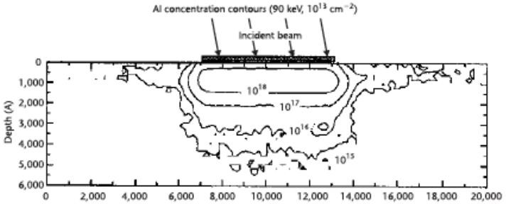
Figure 3.2. The Cross-Sectional Sight of 6H-Silicon-Carbide MESFET.
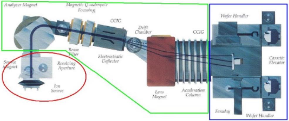
Figure 3.3. The Cross-Sectional Sight of an Ion Implant machine.
In the ion implant machine, the first stage is the source section. In the source section, either the cathode or the anode rods are used to ionized the impurity gas. The second stage is the beamline section, in which the ions are pulled out and quickened in the mass strainer. The third stage is the End-station section, this is the area where the ions are target on the wafer.
The inserter tool scan electrostatically the surface of the wafer to check the evenness of dope. The ion dopant is besieged into the crystals and the molecules cease to move at some profundity at the minuscule level. This is signified by Projected Range (Rp) going from 280Å to 0.10μm. The embedded contamination profile N(x) and the ion amount (Q) is communicated by the equation (3.1) as communicated beneath [72]:
 ………………………………………………………………………………..3.1
In the silicon carbide wafer poly-type, to insert the dopants into the vigorous region of the device ion implantation is most preferable and appropriate method. The fundamental variable to utilize ion implant procedure is to govern ions and have constancy of the ion over the silicon carbide wafer. For mesa separation, the ion implant strategy is picked over the plasma carving. Therefore, the gate spillage current is plus, the execution is enhanced, the resistance of the contacts is dripped, and at last the device has seen a drop in the mobility.
For the box profile, numerous inserts are utilized. The various crease ion implant is portrayed as takes after:
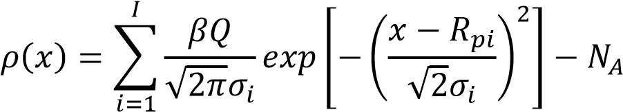 ……………………………………………………………………3.2
The last implant depends on the channel profundity. The figure underneath demonstrates the different ions embeds on 4H-Silicon-Carbide.
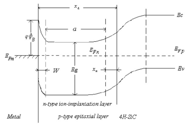
Fig 3.4. The Energy Band of P-type Epitaxial-layer of N-Nitrogen.
For the Silicon Carbide MESFET, the wafer is tempered to execute dissemination of the dope atoms replacement into the range of the cross section of the semiconductor which influence the objective wafers electrical properties. The procedure is done to settle the dilapidation crumbling of the ion implant in the cross section or to conform the film quality developed on the crystal grid.
The annealing procedure for in high-temp furnace. The first step is used the zirconium dioxide apparatus, in which the silicon carbide wafer is fixed. This wafer is paced in the crate of the furnace and the entryway is closed. The second step is the argon gas is allowed to flow at 2.2 SCHF inside the crate of the furnace through gas cleaning system. The third step is to incline the temperature to 318°C in 33min. Now the apparatus is placed for 28min at 318°C. The fourth step is to incline the temperature again to 1210°C in 3hours 20min. After all the apparatus is placed again for 28min at 1210°C. The fifth step is for the last time the temperature is inclined at 1580°C in 2hour 20min, and for last time the apparatus is placed for 11min at 1580°C. The Sixth step is to decline the temperature from 1580°C to 1080°C in 2hours 15min to evade thermal tremor. Still, the temperature is allowed to decline from 1080°C to room temperature for 1hour 25min. At last the wafer is pulled out from the crate at room temperature.
The procedure to obtain a pattern on the positive photoresist S1813 layer over the Silicon Carbide wafer is called photo-lithography. The photo-lithography is used to make connection between the different layers of the integrated circuits. The photo-lithography has different procedure for designing the MESFET on the silicon carbide wafer which is as beneath.
The wafer is heated at 160°C to make the wafer moisture free. The room temperature is kept at 27°C and the humidity of the room should be less than 35%.
- The Spin-Coating of the Photoresist S1813 and HMDS primer.
The HMDS primer is pour on the wafer in ratio of 80:20, and the silicon carbide wafer is placed in the spinner for spin at 3150-3275rpm for 33sec. After the primer, a photoresist S1813 is pour on the silicon carbide wafer, and then it is placed in the spinner for spin at 3150-3275rpm for 32sec.
- The Soft baked and Hard baked of the Silicon Carbide wafer.
In soft baked the silicon carbide wafer is heated at 110°C for 1min 30sec, and in the hard baked the silicon carbide wafer is heated at 125°C for 2min 15sec.
- The Ultra-Violet light used to expose a Photoresist S1813 on the Silicon Carbide wafer.
The first step is to align the mask with the align mark on the silicon carbide wafer. The silicon carbide wafer is transparent. For proper visibility of the mark, the silicon carbide wafer is coated with nickel metallization on the back side. After the alignment of the silicon carbide wafer, the wafer is expose to Ultra-Violet light of the intensity of 365nm for range of time 6 to 12 sec.
- The CD-26 Developer Solution for the Silicon Carbide Wafer.
A developer solution simply remove the photoresist from the portion of the wafer where it is exposed to UV rays. The expose photoresist portion is removed when the wafer is put in the developer solution. If the photoresist is not remove from the expose portion by the developer than re-expose the wafer for long time or increase the intensity of UV rays.
In the etching method, the material is expelled from the silicon carbide wafer. The etching is utilized to expel the unwanted material from the untouched wafer. The etching is done in angstrom. The dry-etch and wet-etch are the two method
There are two sorts of scratching: Wet Etching and Dry Etching. The most well-known kind of solvents for wet scratching procedure is a blend of Hydrogen fluoride arrangement (HF), Nitric corrosive (HNO3) and Acetic corrosive (C2H4O2). The carving rate is dictated by the centralization of every dissolvable.
There are two types of etching: Wet Etching and Dry Etching. The most common type of solvents for wet etching process is a combination of Hydrogen fluoride solution (HF), Nitric acid (HNO3) and Acetic acid (C2H4O2). The etching rate is determined by the concentration of each solvent.
On the other hand, dry etching removes the target atoms by using kinetic energy. In sputtering process plasma etching is used to dislocate the substrate atoms with argon making the target atoms loose. The Wet etching process are explained below:
- The combination of Hydrofluoric acid, Nitric acid and Acetic acid (HNA) generate isotropic etching by redox reaction following the decomposition of silicon dioxide HF acid. The etching rate is 1-3 μm/minute
3 + 4 3 + 18 → 3 2 6 + 8 2 + 4 + 3 ℎ+ + 3 −
- For the silicon dioxide, the BOE maintains a steady etching rate by refilling the depleted floride ions and managing the pH value due to the addition of NH4F to HF.
- Ultra – Etch buffered HF solution is used in the etching process.
- SiO2 is been etched by conc. HF rapidly for meticulous control of the process.
- For more high precision etching, buffered oxide etching (BOE) is preferred at 25°C 2 nm/s 6:1 BOE will etch thermally grown oxide.
- Clean the wafer with acetone.
- Spin-Rinse-Dry (SRD) the wafer.
- 1000 A/min etch rate is obtained for 7:1 BHF
+ 6 → 2 6 + 2 2
- Lower etch rate is recommended to avoid over etching into the substrate.
- Oxidation Process for Silicon Carbide (SiC).
Silicon Oxide (SiO2) is mainly obtained from the constituents of silica. A trace of the silica is found in the volcanic rocks and gemstone. Silicon oxide (SiO2) has two type of structure Crystalline and Amorphous. The sand has amorphous structure of silica and quartz has crystalline structure of the silica. A Silicon Oxide (SiO2) in Amorphous form is used due to bandgap approx. 8.2 eV. In silicon (Si) based device, a thin film of the SiO2 is used as an electrical insulator. In fact, SiO2 is chemically stable compound, and it help as barrier for the impurity diffusion process. Moreover, SiO2 layer help to protect from the atmosphere and package process due to the layer acts like a passivation layers.
A SiO2 thin film grown on the silicon carbide (SiC) substrate. The n-type 4H-SiC substrate can be selected due to the excellent properties like high electron mobility is 800 cm2/Vs, saturated electron velocity is 2×107 cm/s, thermal conductivity is 4.9 W/cmK, and high chemical stability. The main advantage of the 4H-SiC substrate is that it can face high temperature 300oC to 700oC, the wide band approx. 3.23 eV, high breakdown field is 4 MV/cm, and high frequency 75 GHz in the power electronic [80].
On the silicon carbide (SiC) while growing the silicon oxide, carbon (C) is extra element which cause the trouble in growth process. This extra element must be removed during the transition from SiC to SiO2. A high density of the interface trap state degrades the performance with age during the operation period. Now there is need to finding a new procedure of the silicon oxide growth on the Silicon carbide substrate, and need to figure out that the carbon face 4H-SiC or the silicon face 4H-SiC is better. The silicon face 4H-SiC is much better than carbon face 4H-SiC due to it inserts additional carbon in SiO2 [61]. On the other hand, the silicon oxide (SiO2) growth on the carbon face 4H-SiC is more than the silicon face 4H-SiC. This due to the growth variables or the contamination of the carbon. [62].
A research on the oxide layer growth results that near the interface of the oxide layer it seems to be very small. In fact, it is found that near the interface of silicon oxide layer and 4H-SiC substrate are hotspots of interface trap density (Dit). The cause for the formation of the interface density state can be describe by giving valid reason. The first reason is the creation of dandling bond due to vast number of the silicon (Si) atoms. In compare to SiO2/Si framework, the SiC/SiO2 have more dangling bond due to the plenty silicon (Si) atoms. In addition, the second reason is the breaking of bond between carbon and silicon where carbon clusters initiates. Moreover, the breaking of the bond is necessary for the transition from SiC to SiO2. In MOS device, the cluster or the dimers are the part of interface state. It is possible to restrict the interface trap density (Dit)but to some extent. Therefore, the silicon carbide substrate is doped with N-type concentration through ion implantation process. In result, it will reduce the interface trap density (Dit) to some ideal doping concentration. Similarly, the P type concentration is also doped into 4H-SiC to reduce the interface trap density (Dit). The N and P type form a bond with the Silicon (Si) in return the creation C cluster or the dimers are restricted. The last reason is the formation of the interface trap density is not clear yet it could be due to the strain. The interface trap density (Dit) forms during the operation. By post annealing process, the interface trap density (Dit) is not reduced, but by post-oxidation annealing under N2O or POCl3 ambient the interface trap density (Dit) is reduced [98–100].
Presently, there is a need to find out a sustainable technique to grow oxide layer on the Silicon Carbide substrate. Oxidation process is done by two method wet thermal oxidation or Argon (Ar) plasma sputtering process. This are two process commonly used to grow silicon oxide layer (SiO2) on the carbon-face or silicon-face 4H-SiC.
- Growth of SiO2 by Wet Oxidation Process
A n-type 4H-SiC wafers with carbon-face [0 0 0
1̅
] and silicon-face [0 0 0 1] have resistivity approx. 0.02 Ωcm and the carrier concentration is approx. 1018cm-3. The dimension of the wafers is 3-inch diameter and the thickness is 300
μ
m. The silicon carbide (SiC) substrate has imperfection density state in the epitaxial layers due to 8 degree off the axis and inclination toward [1 1 2 0]. Therefore, silicon carbide (SiC) substrate have step bunches in the epitaxial layer. One possessions to be taken under consideration that for the quick and thick silicon dioxide (SiO2) layers wet thermal oxidation growth process is better in compares to the dry oxidation process. Moreover, there is high deformity density in the silicon oxide (SiO2) layers because of the moderate growth rate 1
μ
m/24h respectively. As per our condition, the wet thermal oxidation process has the growth rate 1
μ
m/5.7 h (176 nm/h) for the silicon oxide (SiO2) on the Carbon-face 4H-SiC substrates. The carbon-face and silicon-face 4H-SiC untouched substrate are commonly watched while the
1/2
and
3/4
mono-layer of O2 as native oxide is applied constantly. Before loading samples into furnace, they are altogether cleaned with RCA process to evacuate native oxides and different debasements on the surface of the samples. After the RCA process, the 4H-SiC substrate is inserted in the furnace at initial temperature of 700 oC, and then the temperature rise to 1100 oC at inclination rate of 2oC/min respectively. As shown in figure 4.1, the process is under nitrogen cleanse with stream rate of 4 slm respectively. The dimension of quartz tube, the length is 200 cm and the distance across is 12.5 cm respectively. Inside the furnace, the central zone keeps the temperature 1100 oC while the temperature along the end of tube is 400 oC respectively. The silicon oxide (SiO2) layers is grown on the Carbon-face silicon carbide (C-SiC) substrates with thickness of 320 nm at 1100 oC through the period of 85 minutes. The growth rate of the carbon-face (C-SiC) substrate is more in compare to silicon-face (Si-SiC) substrate. During the silicon oxide growth process, the oxygen at 99 oC is passed through the water bubbler at stream rate of 2 slm respectively. To enhance the growth rate of silicon oxide (SiO2) layer water vapor can pass through which acts like as catalyst.
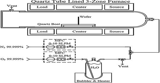
Fig. 4.1. Schematic diagram of wet thermal oxide process
After the silicon oxide (SiO2) layer growth, the oxidation process comes to end. The sample is laid off to come to 700 oC with slow down rate approx. 2 oC/min respectively. In the case of the temperature rise or fall, to keep temperature in control a nitrogen (N2) gas flow at rate of 4 slm. Some times while loading and unloading the wafer the flow rate is double to 8 slm respectively. Now remembering the ultimate objective is to keep the wafer away from flow turbulence in the furnace chamber. It’s important to keep the wafer away because of the contamination. The wafer is gradually and deliberately unloaded from the center of the furnace, thereby maintaining a temperature gradient from 700oC to 25oC and thus having an unloading or loading time of around 10 – 15 min. Moderate loading or unloading wafer maintains a strategic distance from sudden ascent or plunge in the temperature that will minimize thermal stress on the wafer. For the situation of oxidation of Si, the chemical reactions take after for wet and dry oxidations, correspondingly, as given underneath.
Nonetheless, the reaction process might be different for using SiC substrates.
Si + 2H2O → SiO2 + 2H2
Si + O2→ SiO2
Nonetheless, the reaction process might be different for using SiC substrates.
SiC + O2 → SiO + CO,
SiC + 2SiO → 3SiO + CO or
SiC + nO2 → SiO2 + CO (dry) and
SiC + O2 + H2O → SiO2 + CO + 2H2 (wet) [3].
After the growth process, the wafer is annealed under N2 at 1145 oC for 30min. As a post oxidation process is done to enhance the quality. this also reduce the interface trap density state in the MOS device.
4.2. Growth of Silicon Dioxide (SiO2) by Sputtering Technique.
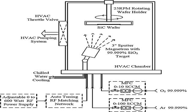
Fig. 4.2. The Schematic diagram of Sputtering Process.
A 3-inch diameter carbon-face and silicon-face 4H-SiC substrate is used to growth silicon oxide (SiO2) layer using RF sputtering technique in Kurt J Lesker sputtering system. In figure 4.2, the schematic diagram of the sputtering process to grow silicon oxide (SiO2) layer. Before the growth of the silicon oxide (SiO2) layer, for several hours the sputtering chamber is kept under vacuum at 10−8 Torr respectively. The Argon (Ar) is used as a sputtering gas in the chamber at flow rate of 15-45 sccm, and the pressure is maintained during the process. To grow 300 nm thick silicon oxide (SiO2) layer, the process is conducted for 3 hours. The RF power is 250 watts and the chamber pressure is maintained at 2.5 mtorr respectively. A small amount of oxygen (O2) is add into the sputter gas in the chamber during silicon oxide (SiO2) molecules to break or partially break from the target to the wafer, and the argon is ionized due to O2. The extra oxygen ions in the chamber reduce the dangling bonds and the potential carriers in the silicon oxide (SiO2) layers. Thus, improve the dielectric strength. Because the sputtering process is a deposition process, rather than a true growth of SiO2 material on the wafer surface. The growth rate on both the Silicon-face and Carbon-faces is almost same, and there is no difference in thickness due to noninvolvement of Cluster. For the uniform growth of the silicon oxide the wafer is rotated at the speed of 25 rpm. The silicon carbide substrate (SiC) is configured to face down during the silicon oxide (SiO2) deposition because it will avoid the unwanted residues on the wafers. In general, the sputtering deposition is not better in matter of quality but it is quite good for the thickness of the layers.
Cite This Work
To export a reference to this article please select a referencing stye below:
Related Services
View all


Related Content
All TagsContent relating to: "Electronics"
Electronics regards the science and technology involved in the development of electrical circuits and electronic devices and equipment that use them.
Related Articles

DMCA / Removal Request
If you are the original writer of this dissertation and no longer wish to have your work published on the UKDiss.com website then please: