Measurement of Radar Pulse Parameters using FFT
Info: 15436 words (62 pages) Dissertation
Published: 11th Jan 2022
Tagged: Computer Science
ABSTRACT
Now a days the threats from the enemy nations has become very high. They might be sending different kinds of signals which are unknown to us. So we need to know the various parameters of the signal to take a counter measure. EM waves are propagated in any medium such as air, water, etc. RADAR transmits a pulse modulated signal with a given pulse width, frequency and PRI depending on the range at which it has to detect the targets. RADAR receives the echo that is reflected from the target and measures the range, velocity and direction of the target. It is required to measure the pulse parameters of the RADAR like pulse width, frequency, amplitude and time of arrival to identify the RADARs from adversaries and to take a counter action by initiating jamming of the RADAR signal to protect ourselves.
The objective of this project is to measure the radar pulse parameters like frequency, amplitude, pulse width and time of arrival of the pulse. FFT is performed on the input signal that is sampled at 105MHz by 14-bit ADC. From the outputs of FFT frequency, pulse width, pulse amplitude and time of arrival of the input signal are found out. This is designed and developed in VHDL language and implemented in Xilinx ISE Design Suite. The outputs are observed using the chipscope pro. The Xtreme DSP kit with virtex-4 FPGA is the hardware that is used for the testing. So using this technique we can measure various parameters of the radar signal.
Key Words: Radar pulse parameters, Fast Fourier Transform, Radar signal processing
CONTENTS
Click to expand Contents
Abbreviations
Chapter-1 Introduction
1.1 Introduction
1.2 Objectives
1.3 Problem Statement
1.4 Proposed Methodology
Chapter-2 Literature Survey
2.1 About Radar Pulse Parameters
2.1.1 Frequency
2.1.2 Amplitude
2.1.3 Time of Arrival
2.1.4 Pulse Width
2.2 Radars
2.3 Fast Fourier Transform
2.3.1 FFT Operation
2.3.2 Butterfly Technique
2.4 Xtreme DSP Kit-iv Key Features
2.4.1 Hardware
2.4.2 Xtreme DSP Kit Key Features
2.5 Clocking Features
2.6 Procedure
2.6.1 Frequency measurement
2.6.2 Pulse width measurement
2.6.3 Time of arrival measurement
2.6.4 Amplitude measurement
CHAPTER-3 Software Implementation of Radar Parameter measurement
3.1 Xilinx Overview
3.1.1 User Interface
3.2 IP Cores
3.2.1 Features of IP Cores
3.2.2 Types of IP Cores
3.3 VHDL
3.3.1 VHDL Design
3.4 Clocking Wizard
CHAPTER-4 Hardware Implementation of Radar Parameter measurement
4.1 Product Description of Xtreme DSP Kit
4.2 Functional Diagram of Xtreme DSP kit
4.3 Physical Layout and Overview of Kit
4.4 Field Programmable Gated Array
4.5 ADCS
4.5.1 Architecture of Adcs
4.5.2 ADC Operation
4.5.3 ADC Clocking
4.6 Bus Structure
4.7 Chip Scope Pro
4.7.1 Product Description
4.7.2 Features of Chip Scope Pro
4.7.3 Functional Description
4.8 DCM module
4.8.1 DCM Module Parameters
CHAPTER-5 Test Setup and Results
5.1 Block Diagram
5.2 Test Setup
5.3 Implementation Results
CHAPTER-6 Conclusion and Future Scope
5.1 Conclusion and Future Scope
References
Annexure
List of Figures
| Figure No. | Name of the Figure | Page No. |
| Figure 2.1
Figure 2.2 |
Butterfly Technique
Xtreme DSP Development Kit-II |
28
29 |
| Figure 3.1 | Clocking Wizard Block Diagram | 39 |
| Figure 4.1 | Functional Diagram Of DSP Kit | 40 |
| Figure 4.2 | DSP Kit Contents | 41 |
| Figure 4.3 | Board Case Front | 42 |
| Figure 4.4 | Board case right side showing USB, Power, JTAG cable | 42 |
| Figure 4.5 | Front View Of DSP Kit-IV | 43 |
| Figure 4.6 | Back View Of DSP Kit-IV | 43 |
| Figure 4.7 | ADC To FPGA Interfacing | 45 |
| Figure 4.8 | Internal Architecture Of ADC | 46 |
| Figure 4.9 | DCM Module Block Diagram | 55 |
| Figure 5.1 | Maximum Frequency Of Bin 0 | 60 |
| Figure 5.2 | Maximum Frequency Of Bin 1 | 60 |
| Figure 5.3 | Maximum Frequency Of Bin 2 | 61 |
| Figure 5.4 | Maximum Frequency Of Bin 3 | 61 |
| Figure 5.5 | Maximum Amplitude of Signal | 62 |
| Figure 5.6 | Pulse width of the Signal | 62 |
List of Tables
| Table No. | Name of the Table | Page No. |
| Table 1 | Bus Structure | 53 |
| Table 2 | DCM Module Parameters | 58 |
| Table 3 | DCM Module I/O Parameters | 60 |
Abbreviations
| PRF | Pulse Repetitive Frequency |
| FFT | Fast Fourier Transform |
| EW | Electronic Warfare |
| ECM | Electronic Counter Measure |
| POI | Probability Of Intercept |
| DIFM | Digits Instantaneous Frequency Measurement |
| ADC | Analog-Digital Converter |
| TOA | Time Of Arrival |
| PW | Pulse Width |
| FPGA | Field Programmable Gated Array |
| SRAM | Static Random Access Memory |
| VIO | Virtual Input / Output |
| VHDL | VHSIC Hardware Description Language |
| PLL | Phase Locked Loop |
| IPCORE | Intellectual Property Core |
| GUI | Graphical User Interface |
| USB | Universal Serial Bus |
Chapter 1 Introduction
1.1 INTRODUCTION
Radar systems use modulated waveforms and directional antennas to transmit electromagnetic energy to a specific volume in space to search for targets. Objects within a search volume will reflect portions of this energy, echoes, back to the radar. These echoes are then processed by the radar receiver to extract target information such as range, velocity, angular position and other target identification characteristics. Radars are most often classified by the types of waveforms they use; it can be continuous wave or pulsed radar. Pulsed radars use a train of pulsed waveforms. In this category, radar systems can be classified on the basis of the pulse repetition frequency (PRF) as low PRF, medium PRF and high PRF radars. Low PRF radars are primarily used for ranging while high PRF radars are mainly used to measure target velocity. The system can be used in many applications those related to detection and identification of targets. As an example, the radar system can be used in autonomous unmanned aircraft systems.
The accurate measurement of radar’s intra pulse parameters in real time is very essential to determine the characteristic of radar signals, which makes it possible to take counter action against the intended radar. First, it is important to determine the primary parameters like frequency, pulse width, amplitude, direction and time of arrival of the radar signals. The analog receiver is capable of measurement of primary parameters but has a limitation of sensitivity, fine accuracy and also resolving time coincidence signals. These limitation being overcome by using the digital receiver, where the parameter extraction happen in frequency domain after fast Fourier transform (FFT) processing. The high sensitivity of the receiver is achieved results of FFT processing gain, accuracy of parameters achieved due to signal processing at higher point FFT and digital receiver presented here will facilitate detection of the radar signal and also provide the range advantage over radar.
ECM Receivers function to search, intercept, locate and identify sources of enemy Electromagnetic radiation. The information they produce is used for the purpose of threat recognition and for the tactical deployment of military forces or assets such as ECM equipment. As the EW scenario is becoming dense day by day, the ECM Receivers are required to process a few million pulses/second for maintaining a high POI (Probability of Intercept). Earlier ECM Receivers have employed analog DIFM (Digital Instantaneous Frequency Measurement) techniques for frequency measurement. DIFM Receivers can only measure a single signal at a time and have a limited pulse processing capability.
The EW scenario today has become very dense and the radar frequency spectrum has become very crowded. Today, many types of Radar are operating very close infrequency range with their signals overlapping in time domain. Hence detection of overlapped pulses and LPI waveforms in presence of noise are the new requirements emerging for ECM Receiver Design. The lack of a prior knowledge about the waveform of interest makes the design of modern Digital ECM Receive very challenging. The availability of high speed ADCs in the GHz range have made direct sampling of signals possible in the IF range. Emergence of high speed FPGAs with dedicated resources for performing DSP operations has enabled implementation of ECM techniques operating in real time. An ADC-FPGA based signal processing architecture was described for Digital Receiver using FFT (Fast Fourier Transform) at low frequency. It presented results for frequency measurement of a100 ns pulse using a Xilinx Logic Core FFT IP for performing 256 point FFT. The Xilinx FFT core has latency in order of μs when configured for 256 point FFT operation. In order to interface with high speed ADC, multiple Xilinx FFT to be used in parallel to achieve the complete throughput without the loss of any input samples.
1.2 OBJECTIVE
This project presents the development of an algorithm for radar pulse signal acquisition and parameters interception. Radar pulse parameters extraction is an important processing stage in the electronic warfare (EW) receivers. The main objective of radar signal parameters measurement is to perform one or more of the following tasks: Signal sorting, to interleave different radar signals and collect pulses of each individual radar; signal identification, to classify the radar types from the collected pulses and radar parameters extraction, to measure unknown radar parameters when only single radar is available in the concerning frequency band .So with this technique we can find the unknown pulse parameters as frequency, amplitude, pulse width and time of arrival.
1.3 PROBLEM STATEMENT
We have threats from unknown transmitters they send signals of unknown parameters. So we need to calculate the parameters of the radar signals. Using the digital receiver we can quantize the values and evaluate the approximate.
1.4 PROPOSED METHODOLOGY
We are using the FFT in evaluating the signal characteristics and for calculating the parameters in a digitized domain. Performance based hardware with specific outcomes is used as a helping module.
Chapter 2 Literature Survey
2.1 ABOUT RADAR PARAMETERS
The parameters to be measured are Frequency, Amplitude, Pulse Width and Time of Arrival.
2.1.1 FREQUENCY
Frequency of the radar signal is one of the important basic parameters measured by ECM receiver. By comparing the frequency of the pulses received, pulse trains of various radars can be sorted out. To make the jamming and others important actions very effective, better frequency resolution and accuracy are desirable specifications of the receiver. In an electronic warfare scenario, it is required to intercept and resolve multiple radar emitters operating at the same time. So, in order to achieve simultaneous signal resolving capability, FFT is selected as the frequency measurement technique. The input frequency of the signal after normal FFT spectrum analysis is given in Eqn.
Measured Frequency =fs/N*k
Where fs the sampling frequency and k is the index corresponding to the maximum FFT bin and N is number of points of FFT.
2.1.2 AMPLITUDE
The amplitude of the intercepted radar signal is measured from the FFT spectrum. The data input from the ADC is 14 bit, it is fed to FPGA for 256 points FFT computation. The FFT output i.e. the magnitude spectrum will be 23 bits real and 23 bits imaginary data. The peak value of real and imaginary FFT output is squared and the square root of the sum of these values is used to find the absolute peak amplitude. The PA parameter is computed by taking the peak value of the processed data in a given pulse. It can be used to generate the scan pattern of some radar, a sorting parameter to predict the scan pattern of radar, and predict radar to an EW receiver approximate range. Accurate pulse amplitude measurement may be helpful in generating some effective range estimation that can be used in different applications.
2.1.3 PULSE WIDTH
Pulse width is the envelope of the intercepted RF signal. The accurate measurement of pulse width is required to identify the type of radar, whether it is surveillance, tracking or missile homing radar. Accurate PW measurement is achieved with precise knowledge of leading edge and trailing edge of the pulse.PW is an unreliable sorting parameter because of multipath transmission problem. PW can range from few nanoseconds to continuous wave (CW). In most receivers, maximum PW is programmable (that is, a short pulse is measured with fine time resolution whereas long pulse is measured with coarse time resolution). In the early years, a pulse is passed through a high pass filter, this results in a positive spike at leading edge and a negative spike at the trailing edge. By using the positive spike to start count and the negative spike to stop the count the PW can be measured with a great accuracy.
2.1.4 TIME OF ARRIVAL
Time of arrival (TOA) measurement is required to get the PRF of the intercepted radar signals. For TOA calculation, a free running counter of 5 MHz is implemented in FPGA. Whenever there is a signal present, first frame of FFT is used for generating the TOA strobe. At the leading edge of the TOA strobe, the counter value will be registered. The counter value multiplied by the resolution of TOA will yield TOA measurement. The range of TOA varies from 1 ns to 20ms, which results PRF from 50 Hz to 1 Million pulses per second. TOA can be used to generate the pulse repetition interval. It provides a time reference to all of the received pulses. Also it can be used to interrupt the processor to begin data acquisition phase.
2.2 Radars
There are different types of radars in our EW:
- Early Warning (EW) Radar Radar Systems
- Target Acquisition (TA, TAR) Radar Systems
- Surface-to-Air Missile (SAM) Systems
- Anti-Aircraft Artillery (AAA) Systems
- Surface Search (SS) Radar Systems
- Surface Search Radar
- Coastal Surveillance Radar
- Harbour Surveillance Radar
- Antisubmarine Warfare (ASW) Radar
- Height Finder (HF) Radar Systems
- Gap Filler Radar Systems
2.2.1 Detection And Search Radars
Search radars scan a wide area with pulses of short radio waves. Usually scan the area two to four times per minute. The waves are usually less than one meter long. Ships and planes are made of metal and reflect the radio waves. The radar measures the distance to the reflector by measuring the time of the return of the emission of a pulse to the reception, dividing this by two, and then multiplying by the speed of light. To be accepted, the pulse received must be within a period of time called the range gate. Radar determines direction because short radio waves behave as a search light when emitted from the reflector of the radar antenna.
2.2.2 Targeting Radars
Orientation radars use the same principle, but scan a much narrower area much more frequently, usually several times per second or more, where a search radar can scan more widely and less frequently. The missile block describes the scenario in which an orientation radar has acquired a target and the fire control can calculate a path for the missile towards the target; In semiautomatic systems of homing radar, this implies that the missile can “see” the target that the orientation radar is “illuminating”. Some guidance radars have a range gate that can track a target, to eliminate clutter and electronic countermeasures.
2.3 Fast Fourier Transform
A strong>fast Fourier transform (FFT) algorithm computes the discrete Fourier transform (DFT) of a sequence, or it’s inverse. Fourier analysis converts a signal from its original domain (often time or space) to a representation in the frequency domain and vice versa. An FFT rapidly computes such transformations by factorizing the DFT matrix into a product of sparse (mostly zero) factors As a result, it manages to reduce the complexity of computing the DFT from {displaystyle O(n^{2})}, which arises if one simply applies the definition of DFT, to {displaystyle O(nlog n)}, where {displaystyle n}is the data size. Fast Fourier transforms are widely used for many applications in engineering, science, and mathematics. There are many different FFT algorithms involving a wide range of mathematics, from simple complex-number arithmetic to group theory and number theory. The DFT is obtained by decomposing a sequence of values into components of different frequencies.
This operation is useful in many fields. But computing it directly from the definition is often too slow to be practical. An FFT is a way to calculate the same result more quickly: calculate the DFT of N points in the naive manner, using the definition, take O (N2) arithmetic operations, whereas an FFT can calculate the same DFT in only O Log N). The speed difference can be huge, especially for long datasets where N can be in the thousands or millions. In practice, the calculation time can be reduced by several orders of magnitude in such cases, and the improvement is approximately proportional to N log N. This great improvement made the DFT calculation practical; FFTs are of great importance for a wide variety of applications, from digital signal processing and solving partial differential equations to algorithms for quick multiplication of large integers.
The best-known FFT algorithms depend upon the factorization of N, but there are FFTs with O(N log N) complexity for all N, even for prime N. Many FFT algorithms only depend on the fact that {displaystyle e^{-2pi i/N}}is an N-th primitive root of unity, and thus can be applied to analogous transforms over any finite field, such as number-theoretic transforms. Since the inverse DFT is the same as the DFT, but with the opposite sign in the exponent and a 1/N factor, any FFT algorithm can easily be adapted for it.
2.3.1 FFT Operation
FFT is a complicated algorithm, and its details are often left to those who specialize in such things. This section describes the general operation of the FFT, but faces a key issue: the use of complex numbers. If you have a background in complex math, you can read between the lines to understand the true nature of the algorithm. Do not worry if the details elude you; few scientists and engineers using the FFT could write the program from scratch.
In complex notation, the time and frequency domains contain a signal composed of N complex points. Each of these complex points consists of two numbers, the real part and the imaginary part. For example, when we talk about the complex sample X [42], it refers to the combination of ReX [42] and ImX [42]. In other words, each complex variable has two numbers. When two complex variables are multiplied, the four individual components must be combined to form the two components of the product. The following discussion on “How FFT works” uses this complex notation jargon. That is, the singular terms: signal, point, sample and value, refer to the combination of the real part and the imaginary part.
The FFT operates by decomposing a time domain signal of N points into N time domain signals composed of each of a single point. The second step is to calculate the N frequency spectra corresponding to these N time domain signals. Finally, N spectra are synthesized in a single frequency spectrum. The FFT is a fast algorithm, O [NlogN] to calculate the Discrete Fourier Transform (DFT), which naively is a calculation of O [N2]. The DFT, as the most familiar continuous version of the Fourier transform, has a direct and inverse shape that is defined as follows:
Forward Discrete Fourier Transform (DFT):
n=0 -i2πkn / N
Xk= ∑ xn e
N-1
Inverse Discrete Fourier Transform (IDFT):
K=0 i2πkn / N
xn=1/N ∑ Xk e
N-1
The transformation of xn → Xk is a translation of the configuration space into frequency space, and can be very useful both in the scanning of the power spectrum of a signal and in transforming certain problems for a more efficient calculation.
2.3.2 Butterfly Technique
In the context of fast Fourier transform algorithms, a butterfly is a portion of the computation that combines the results of smaller discrete Fourier transforms (DFTs) into a larger DFT, or vice versa (breaking a larger DFT up into sub transforms). The name “butterfly” comes from the shape of the data-flow diagram in the radix-2 case. The smaller DFTs are then combined via size-r butterflies, which themselves are DFTs of size r (performed m times on corresponding outputs of the sub-transforms) pre-multiplied by roots of unity (known as twiddle factors). (This is the “decimation in time” case; one can also perform the steps in reverse, known as “decimation in frequency”, where the butterflies come first and are post-multiplied by twiddle factors
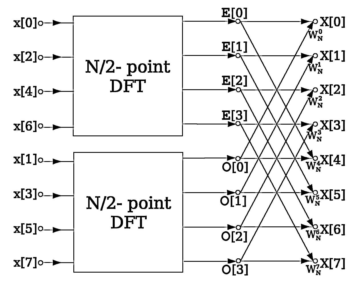
Figure 2.1: Butterfly Technique
2.4 Xtreme DSP Development Kit-IV Key Features
The Xtreme DSP Development Kit-IV serves as an ideal development platform for Virtex-4 FPGA technology and provides input into the scalable DIME-II systems available from Nalla tech. Its high-performance dual-channel ADCs and DACs, as well as the user-programmable Virtex-4, are ideal for deploying high-performance signal processing applications such as Software Defined Radio, 3G Wireless, Networking, HDTV or Video Imaging. With the help of this Xtreme DSP kit we are doing the project. So the key features of this DSP kit are:
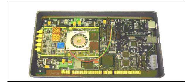
Figure 2.2: Xtreme DSP Development kit-II
The key features of the Kit include:
2.4.1 Hardware
Xtreme DSP development board consisting of a motherboard with a module (daughter card) in a separate blue case. The motherboard is referred to as the “Ben ONE-Kit Motherboard “and the module is named” Ben ADDA DIME-II module “.
- Ben ONE-Kit motherboard
- Supports only the supplied Ben ADDA DIME-II module
- Spartan-II FPGA for 3.3V / 5V PCI or USB interface
- Host interfaces via 3.3 V / 5 V PCI PCI 32-bit / 33 MHz interfaces or USB v1.1
- Status LED
- JTAG configuration headers
- 0.1 “pitch headers directly connected to user-programmable FPGA I / O
- Ben ADDA DIME-II Module
- Virtex-4 FPGA User: XC4VSX35-10FF668
- 2 independent ADC channels: AD6645 ADC (14 bits up to 105 MSPS)
- 2 independent DAC channels: AD9772 DAC (14 bits up to 160 MSPS) • Support for external clock, on-board oscillator and programmable clocks
- ZBT-SRAM banks (133MHz, 512Kx32 bits per bank)
2.4.2 XtremeDSP Development Kit-IV User Guide
- Multiple sync options: Internal and External
- Status LED
- External power supply (US network cable with separate UK, European or Australian network adapters)
- Wide input (90 – 264Vac), multiple output, power supply, generation;
- +5 Volts at 5 A, + 12 Volts at 2 A, -12 Volts at 800 mA
- Compatible USB cable v1.1, 2 meters long
- 5 MCX to BNC cables for connection to ADC / DAC connectors and external clock
- Rear PCI plate and 2 screws
- 2x BNC jack to jack adapter for use in loopback configurations
- Large blue carrying case
Xtreme DSP Installation Pack containing
- Nalla tech FUSE (Field upgradeable system environment) Software CD. It provides the ability to control and configure FPGAs and provides facilities for transferring data between the Kit and a host PC through a GUI or a C-based API.
- Nalla tech Xtreme DSP Development Kit-IV CD that provides documentation on Nalla tech hardware as well as hardware support files for use in the Falla Nalla technology environment
- Optional Nalla technology evaluation software.
2.5 Clocking Features
The main functional features related to the clock, desired and specified, can be used by the wizard to select an appropriate primitive. Incompatible functions are automatically dimmed to help the designer evaluate feature offsets. Synchronization features include:
- Frequency Synthesis
- Phase Alignment
- Widespread Spectrum
- Output Jitter Minimization
- Larger input jitter allowance
- Minimizing power
- Dynamic phase change
- Dynamic reconfiguration
- Start and sequencing of the secure clock
- Clock monitoring
- Primitive Auto
- Automatic buffering
- Matched routing
Input clocks
An input clock is the default behavior, but two input clocks can be selected by selecting a secondary clock source. Only the timing parameters of the input clocks are required in their specified units; The wizard uses these parameters as needed to set output clocks.
Input clock instability option
The wizard allows you to specify the input clock jitter on UI or PS units using a drop-down menu.
Watches
The number of output clocks is configurable by the user. The maximum number allowed depends on the device or primitive selected and on the interaction of the main synchronization features that you specify. For MMCM (E2 / E3) you can configure up to seven, PLLE2 maximum six and PLLE3 maximum two output clocks. If the selected primitive is Auto, then all seven output clocks can be configured. Enter the desired timing parameters (frequency, phase and duty cycle) and let the synchronization wizard automatically select and configure the synchronization primitive and the network to meet the requested characteristics. If it is not possible to comply exactly with the requested parameter settings due to the number of available input clocks, the best attempt settings are provided. When this is the case, the clocks are sorted so that clk_out1 is the highest priority clock and is more likely to meet the requested timing parameters. The wizard prompts you for frequency parameter settings before the phase and duty cycle settings.
Clock Buffer and Comments
In addition to configuring the synchronization primitive within the device, the wizard also helps build the synchronization network. Intermediate storage options are provided for input and output clocks. The feedback from the primitive can be controlled by the user or left to the wizard to connect automatically. If automatic feedback is selected, the feedback path coincides with the timing of clk_out1.
Optional Ports
All primitive ports are available for user configuration. You can expose any of the ports in the synchronization primitive, and these are also provided in the source code.
Primitive override
All configuration parameters are also configurable by the user. In addition, if a given value is undesirable, any of the calculated parameters can be overridden with the desired settings.
Clock display
The Clock Monitor function allows you to monitor the clocks on a system, normally
MMCM / PLL. This detects the change in the clock frequency, a clock failure or a clock
Having.
Clock Stop
The Clock Stop goes high when the clock is flat-lined for more than 50 clock cycles.
Clock Glitch
The Clock Monitor can detect the glitch in the user clock. The minimum glitch it can detect in the user clock is one clock period of the reference clock.
Note: The Clock Glitch condition may overlap with the Clock Overrun.
Clock Out of Range
The Clock Monitor detects if the user clock frequency exceeds or goes down the required frequency.
Note: Clock under run signal may also go high during the stop condition, if the frequency of the signals goes much lower than the desired frequency.
Auto Primitive
This feature helps instantiating the clocking primitive which exactly fits into your requirements with minimum utilization of clocking resources, high performance and better clock routing. All clocking features and optional ports would be in unselected state when you select primitive as Auto. You need to exclusively enable the options which are required.
2.6 PROCEDURE
The unknown signal received from the radar receiver is connected to the input ADC port of the Xtreme DSP development board. The inbuilt ADC on the board produces a digital data of 14 bit width and it works with a clock of 105MHz. The output of the ADC is in 2’s compliment form. This output is given as the real input to the FFT IP core in the FPGA processor. FFT IP core performs radix-2 DIT Fast Fourier transform and produces the output data. The output data width produced depends upon the no. of samples in the FFT. The output data consists of both real and imaginary outputs. The complex magnitude of the output data is calculated.
The complex magnitude of all the samples is compared and the maximum magnitude is found. This maximum magnitude is the amplitude of the signal received. The index at the maximum magnitude is the bin number used to find out the frequency of the received signal. The frequency is calculated using the following formula
F(received)=bin_no *(Fs/N)
The pulse width of the received signal is calculated by counting the total no of execution cycles while the bin number is greater than zero. Multiplying the frame interval with the total number gives the pulse width of the received signal. Subtracting the single frame interval from the total time taken before the first frame execution gives us the time of arrival of the signal.
2.6.1 Frequency Measurement:
FFT is performed on the input signal and the results of FFT are compared for bins having maximum magnitude. The index of the bin no. that has maximum amplitude is used to calculate the frequency as
F(o/p)= m . fs/N
where,
m 0 to N-1; output index
fs Sampling Frequency
N no . of i/p samples.
2.6.2 Pulse width Measurement:
Using FFT, pulse width of incoming signal will be measured .For every N i/p samples FFT IP core gives a done signal for one clock cycle. Counting the number of occurrences of done signal when the bin no. is having the same frequency as given at i/p gives the pulse width in terms of FFT frame width is
PW= N * ts
where,
ts Sampling Time.
Ex: Pulse width count = 3.
Final pulse width = 3* Frame width.
2.6.3 Time of Arrival Measurement:
Again usingthe done signal TOA of the input signal can be found out. By the time done signal becomes high one set of i/p samples have already came i,e, one frame of i/p samples have elapsed i,e, the signal has already arrived. From the done signal, also checking the bin no. for required one, a free running counter of width greater than the maximum PRI i,e Pulse Repetition Frequency to be measured is chosen for TOA measurement. From the value of their counter at the occurrence of done signal frame width is subtracted to get the TOA.
TOA = {Counter value @ done signal} – Frame width
2.6.4 Amplitude Measurement:
The magnitude of the bin having maximum amplitude is nothing but the amplitude of the i/p signal.
Chapter 3 Software Implementation
3.1 XILINX OVERVIEW
Xilinx Tools is a set of software tools that are used to design digital circuits implemented using the Xilinx Field Programmable Gate Array (FPGA) Complex Programmable Logic Device (CPLD). The design procedure consists of: a) the design, b) the synthesis and execution of the design, c) the functional simulation and d) the tests and verifications. Digital designs can be introduced in a number of ways using the above CAD tools: using a schematic input tool, using a hardware description language (HDL) – Verilog or VHDL or a combination of both. In this lab we will only use the design flow that involves the use of Verilog HDL. CAD tools allow you to design combinational and sequential circuits beginning with Verilog HDL design specifications. The steps in this design procedure are listed below:
- Create the Verilog design input file using the template editor.
- Compile and implement the Verilog design file (s).
- Create the test vectors and simulate the design (functional simulation) without using PLD (FPGA or CPLD).
- Assign input / output pins to implement the design on a target device.
- Download the bit stream to an FPGA or CPLD device.
- Test Design on the FPGA / CPLD Device
A Verilog input file in the Xilinx software environment consists of the following segments:
Header: module name, list of input and output ports.
Declarations: ports of entry and exit, registers and cables.
Logical descriptions: equations, state machines and logical functions.
End: end module All designs for this laboratory must be specified in the previous Verilog input format.
Note that the status diagram segment does not exist for ISE® combinational logic designs.
3.1.1 USER INTERFACE:
The main user interface of the ISE is the Project Navigator, which includes the design hierarchy (Sources), a source code editor (Workplace), an output console (Transcript) and a Processes tree.
The design hierarchy consists of design files (modules), whose dependencies are interpreted by the ISE and are displayed as a tree structure. For single-chip designs there may be a main module, with other modules included in the main module, similar to the main () subroutine in C ++ programs. Design constraints are specified in modules, which include pin configuration and mapping.
The Processes hierarchy describes the operations that the ISE will perform on the active module. The hierarchy includes compilation functions, their dependency functions, and other utilities. The window also denotes problems or errors that arise with each function.
The Transcript window provides the status of the currently executing operations and informs engineers about design problems. Such problems can be filtered to show warnings, errors, or both.
3.2 IP CORE:
In electronic design, a semiconductor IP core, IP core, or IP block is a reusable unit of logical design, cell or integrated circuit (commonly called a “chip”) that is the intellectual property of a party. IP cores may be licensed elsewhere or may be owned and used by a single party. The term is derived from the license of the copyright of patents and / or source code that exist in the design. IP cores can be used as building blocks within application-specific integrated circuit designs (ASICs) or Field Programmable Logic Designs (FPGAs).
The core of the LogiCORE IP Synchronization Wizard simplifies the creation of HDL source code wrappers for custom clock circuits based on your synchronization requirements. The wizard guides you in setting the appropriate attributes for your synchronization primitive and allows you to override any parameters calculated by the wizard. In addition to providing an HDL wrapper to implement the desired synchronization circuit, the Synchronization Wizard also provides a summary of the timing parameters generated by the Xilinx synchronization tools for the circuit.
3.2.1 Features
Selection of mixed mode clock (MMCM) / phase locked loop (PLL) primitives. GUI options are enabled for supported functions for primitives.
The safe start of the clock function allows a stable and valid clock at the output. Activation of sequencing provides sequenced output clocks.
Accepts up to two input clocks and up to seven output clocks per watch network.
Provides an AXI4-Lite interface to dynamically reconfigure synchronization primitives to multiply, divide, phase or work cycle.
Automatically configures the synchronization primitive based on the selected synchronization characteristics.
Automatically calculates the voltage-controlled oscillator (VCO) frequency for primitives.
Clocking features include:
Frequency Synthesis:
This feature allows the output clocks to have different frequencies than the active input clock.
Dispersion Spectrum:
This feature provides modulated output clocks that reduce the spectral density of electromagnetic interference (EMI) generated by electronic devices. This function is available only for the ADV MMCM (E2 / E3) primitive. The UNISIM simulation support for this function is not available in the current version.
Phase Alignment:
This feature allows the output clock to be synchronized in phase with a reference, such as the input clock pin of a device.
Minimize power:
This minimizes the amount of energy needed for the primitive with the possible expense of frequency, lag or precision of the work cycle.
Dynamic Phase Shift:
This feature allows you to change the phase ratio on the output clocks.
Dynamic Reconfiguration:
This feature allows you to change the programming of the primitive after device configuration. When this option is selected, the AXI4-Lite interface is selected by default to reconfigure the synchronization primitive.
Balanced:
Selection of balanced results in the software, selecting the correct bandwidth to optimize the jitter.
Minimize output jitter:
This feature minimizes jitter in the output clocks, but at the expense of the power and possibly the output clock phase error. This function is not available with ‘Maximize input jitter filtering’.
Maximize input jitter filtering:
This feature allows greater input jitter on the input clocks, but can negatively affect the jitter on the output clocks. This function is not available with ‘Minimize output jitter’.
Start-up and sequencing of the safe clock:
This function is useful for obtaining a stable and valid clock at the output. It also enables the clocks in a particular sequence order as specified in the configuration.
Clock Monitor:
This feature helps you monitor the clock inputs to the Synchronization Wizard. It can control up to 4 clocks. It can monitor if the input frequency is outside the range of the expected frequency, detect the clock stop and the clock failures.
Primitive Auto:
When selecting this primitive instance the synchronization primitive suitable for your needs. It is not necessary to know the MMCM or PLL specification to judge which primitive fits your needs.
3.2.2 TYPES OF IP CORES:
The IP core can be described as being for chip design what a library is for computer programming or a discrete integrated circuit component is for printed circuit board design.
Soft cores:
IP cores are typically offered as synthesizable RTL. Synthesizable cores are delivered in a hardware description language such as Verilog or VHSIC hardware description language (VHDL). These are analogous to High-level languages like C in the field of computer programming. IP cores delivered to chip makers such as RTL enable chip designers to modify designs (at a functional level), although many IP providers do not offer warranty or support for modified designs.
IP kernels are also sometimes offered as generic gate-level netlists. The netlist is a Boolean algebra representation of the logic function of the IP implemented as generic gateways or process-specific standard cells. An IP core implemented as generic ports is portable to any process technology. A gate-level netlist is analogous to an assembly code list in the field of computer programming. A netlist provides the primary IP provider reasonable protection against reverse engineering. Both netlist and synthesizable cores are called “soft cores,” since they both allow a flow of synthesis, location, and path (SPR) design.
Hard cores:
Hard cores, by the nature of their low-level representation, offer better predictability of chip performance in terms of performance and time area. Analog and mixed-signal logic is generally defined as a lower-level physical description. Therefore, the analog IP (SerDes, PLLs, DAC, ADC, PHYs, etc.) are provided to chip manufacturers in transistor-layout format (such as GDSII). Digital IP kernels are sometimes offered in layout format, too.
Such cores, whether analog or digital, are called “hard cores” (or hard macros), because the kernel application function cannot be significantly modified by chip designers. Transistor designs must obey the design rules of the destination casting process and therefore the hard cores supplied for the casting process cannot easily be transferred to another process or cast. Trader smelter operators (such as IBM, Fujitsu, Samsung, TI, etc.) offer a variety of hard macro IP functions built for their own casting process, helping to ensure customer blocking.
3.3 VHDL
VHDL (hardware description language VHSIC) is a hardware description language used in electronic design automation to describe digital and mixed signal systems such as field programmable gate arrays and integrated circuits. VHDL can also be used as a general-purpose parallel programming language.
3.3.1 VHDL Design
VHDL is commonly used to write text models that describe a logic circuit. Such a model is processed by a synthesis program only if it is part of the logical design. A simulation program is used to test the logical design using simulation models to represent logic circuits that interfere with the design. This collection of simulation models is commonly referred to as the test bench.
A VHDL simulator is typically an event driven stimulator. This means that each transaction is added to an event queue for a specific scheduled time. The zero delay is also allowed, but still needs to be programmed: Delta delays are used for these cases, representing an infinitely small time step. The simulation alters between two modes: the execution of instructions, where the activated statements are evaluated and the processing of events, where the events in the queue are processed.
VHDL has constructs to handle the parallelism inherent in hardware designs, but these constructs (processes) differ in syntax from parallel constructs in Ada (tasks). Like Ada, VHDL is heavily typed and does not case-sensitive. In order to directly represent the operations that are common in hardware, there are many VHDL features not found in Ada, such as an extended set of Boolean operators, including nand and nor. VHDL also allows matrices to be indexed in an up or down direction; Both conventions are used in hardware, while in Ada and most programming languages only indexing is up.
VHDL has file input and output capabilities and can be used as a commonly used language for word processing, but files are most commonly used by a simulation test bench for stimulus or verification data. There are some VHDL compilers that create executable binaries. In this case, it might be possible to use VHDL to write a test bench to verify the functionality of the design using files in the central computer to define stimuli, interact with the user and compare the results with those expected.
Hardware can be designed in a VHDL IDE (for FPGA implementation such as Xilinx ISE, Altera Quartus, Synopsys Synplify or Mentor Graphics HDL Designer) to produce the RTL scheme of the desired circuit. After that, the generated scheme can be verified using simulation software that shows the waveforms of inputs and outputs of the circuit after generating the appropriate test bench. To generate an appropriate test bench for a particular circuit or VHDL code, the inputs must be correctly defined.
One endpoint is that when a VHDL model translates to “gates and cables” that are assigned to a programmable logic device such as a CPLD or FPGA, then it is the actual hardware being configured, rather than the VHDL code being ” Executed “as if in some form of a processor chip.
3.4 CLOCKING WIZARD
The LogiCORE ™ IP Clocking Wizard generates HDL source code to configure a clock circuit according to user requirements. The wizard can automatically select a suitable synchronization primitive or configure the temporary storage, feedback, and timing parameters for a synchronization network or help the user configure the attributes of a manually selected primitive. If desired, the user can also override any parameter calculated by the wizard. In addition to generating HDL source for the clock circuit, the wizard also invokes the Xilinx synchronization analysis tools to generate a time parameter report.
Key Features & Benefits
- Accepts up to two input clocks and up to seven output clocks per watch network
- Automatically chooses the correct sync primitive for a selected device and configures the synchronization primitive based on the user-selected synchronization characteristics
- Calculates the VCO frequency for primitives with an oscillator, and provides multiplication and division values based on the input and output frequency requirements
- Implements a general configuration that supports phase change and duty cycle requirements
- Provides the ability to override a self-selected clock primitive, as well as any calculated attribute
- Provides extended spectrum sync support.
- Optionally, buffering clock signals.
- Provides time estimates for the clock circuit as well as parameters that can be entered into the Xilinx Power Estimator (XPE) for energy consumption calculations.
Clocking Wizard helps create the clocking circuit for the required output clock frequency, phase and duty cycle using mixed-mode clock manager (MMCM)(E2/E3) or phase-locked loop (PLL)(E2/E3) primitive. It also helps verify the output generated clock frequency in simulation, providing a synthesizable example design which can be tested on the hardware. It also supports Spread Spectrum feature which is helpful in reducing Electromagnetic Interference.
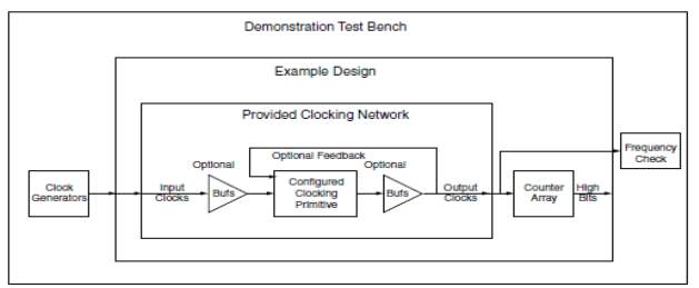
Figure 3.1: Clocking Wizard Block Diagram
Chapter 4 Hardware Implementation
4.1 PRODUCT DESCRIPTION
The Xtreme SP Development Kit, developed in collaboration with Nalla tech, the FPGA computing solution solution, provides a complete platform for high-performance signal processing applications such as Software Defined Radio, 3G Wireless, Networking, HDTV and Video Imaging. This kit features high performance dual channel ADCs and DACs, a user programmable Virtex-4 FPGA, and is fully supported by Xilinx System Generator for Hardware simulation.
4.2 Xtreme DSP Development Kit-IV Functional Diagram
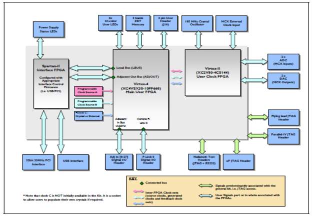
Figure 4.1: Functional diagram of DSP kit
The Xtreme DSP Development Kit-IV includes three Xilinx FPGAs:a Virtex-4 User FPGA, a Virtex-II FPGA for clock management and a FPGA Spartan-II Interface. The Virtex-4 device is available exclusively for the user’s designs while the Spartan-II comes preconfigured with the firmware for PCI / USB interconnect. The PCI / USB interconnect firmware and low level drivers summarize the user’s PCI / USB interface, resulting in a simplified design process for user designs / applications. The FPGA interface communicates directly with the largest user FPGA (XC4VSX35-10FF668) via a dedicated communications bus that is made up of the LBUS and ADJOUT buses.
The Virtex-4 XC4VSX35-10FF668 device is intended to be used for the main part of a user’s design.
4.3 PHYSICAL LAYOUT
OVERVIEW OF XTREME DSP KIT IV
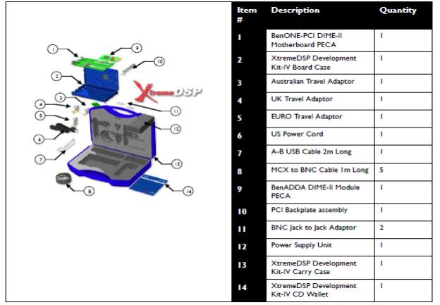
Figure 4.2: Kit contents
Figure 4.3: Board case Front
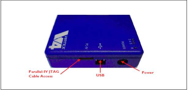
Figure 4.4: Board case right side showing USB, Power, JTAG cable access
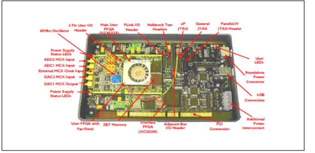
Figure 4.5: Front view of DSP kit IV
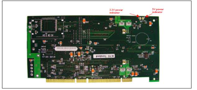
Figure 4.6: Back view of DSP kit IV
4.4 Field Programmable Gated Array
A field–programmablegatearray (FPGA) is an integrated circuit designed to be configured by a customer or a designer after manufacturing – hence “field-programmable“. The FPGA configuration is generally specified using a hardware description language (HDL), similar to that used for an application-specific integrated circuit (ASIC). (Circuit diagrams were previously used to specify the configuration, as they were for ASICs, but this is increasingly rare.)

FPGAs contain an array of programmable logic blocks, and a hierarchy of reconfigurable interconnects that allow the blocks to be “wired together”, like many logic gates that can be inter-wired in different configurations. Logic blocks can be configured to perform complex combinational functions, or merely simple logic gates like AND and XOR. In most FPGAs, logic blocks also include memory elements, which may be simple flip-flops or more complete blocks of memory.
4.4.1 FPGA Design
Field programmable gate arrays (FPGAs) have large gateway and RAM block resources to implement complex digital calculations. As FPGA designs employ very fast I / O and bidirectional data buses, it becomes a challenge to verify the correct time of valid data within configuration time and waiting time. Plant planning allows the allocation of resources within FPGAs to meet these time constraints. FPGAs can be used to implement any logical functions that an ASIC could perform. The ability to update functionality after shipment, partial reconfiguration of a part of the design, and low non-recurring engineering costs in relation to an ASIC design offer advantages for many applications.
Some FPGAs have analog functions as well as digital functions. The most common analog feature is the programmable rotational speed at each output pin, which allows the engineer to set low speeds on slightly charged pins that would otherwise unacceptably touch or engage and set higher speeds on very charged pins on channels High-speed than otherwise Very slow running Quartz crystal oscillators, on-chip capacitor resistance oscillators, and phase loops with controlled voltage oscillators are also common for generating and managing the clock and For the serializer-deserializer of high speed (SERDES).
4.5 ADCS
The Ben ADDA DIME-II module used in the Xtreme DSP Development Kit-IV has two analog input channels, with each channel providing independent data and control signals to the FPGA. Two 14-bit wide data sets are fed from two ADC devices (AD6645), each of which has an isolated supply and ground plane.
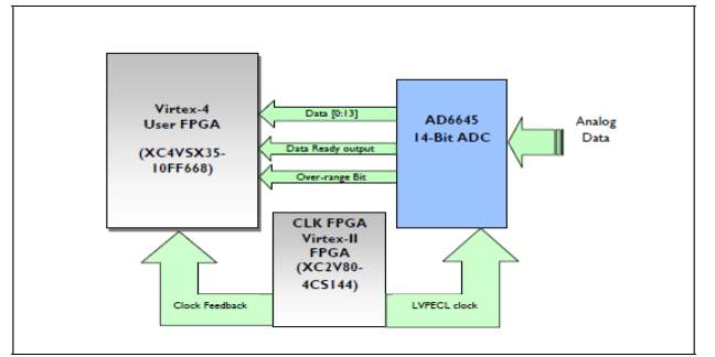
Figure 4.7: ADC to FPGA Interface
As the need for data bandwidth for end systems increases, data rates continue to increase for the analog-to-digital (ADC) converters and the FPGA solution associated with the interface with the ADCs and other parts of the system. Manufacturers of ADCs and FPGAs have responded with faster and more capable devices at a lower cost.
The main characteristics of on-board ADC channels are:
- 14 – bit ADC resolution, 2 – bit add – on format.
- Sample data rate of 105MSPS.
- Analog impedance analog inputs of 50 ohms or with differential input of population changes.
- 3rd order filter on analog inputs (-3dB 58MHz point).
- ADCs were recorded differentially.
4.5.1 ARCHITECTURE:
The ADC (AD6645) is straightforward to operate – the user is only required to apply data and a clock input. There are no set-up or control signals.
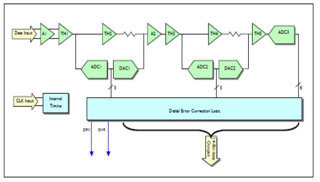
Figure 4.8: Internal architecture of ADC
4.5.2 Theory of ADC (AD6645) Operation
The AD6645 has complementary analog inputs; Each input is centered at 2.4V and should oscillate +/- 0.55V around this 2.4V reference. This means that the differential analog input signal will be 2.2Vpp, since both input signals (AIN and AIN #) are offset 180 degrees from each other. When the data reaches the AD6645, both analog inputs are buffered before the first track and hold (TH1). Analog signals are maintained in TH1 while the ENCODE (CLK) pulse is high and then data is applied to the input of a thick 5-bit ADC (ADC1). The digital output of ADC1 is input to the 5-bit DAC1. The output of the DAC1 is subtracted from the delayed analog signal at the TH3 input to generate a first residue signal. The purpose of TH2 is to provide a channel delay to compensate for the digital delay of ADC1.
This first residue signal is then applied to the second conversion stage. Again a similar process is achieved through this step, which eventually leads to obtaining a second residue signal which is applied to a third 6-bit ADC. Finally, the digital outputs of ADC1, ADC2 and ADC3 are added and corrected in the digital error correction logic to generate.
Analog ADC Inputs
The inputs of the ADC devices are connected via MCX connectors on the front of the module. The standard configuration sent shows single-ended 50Ω inputs, each with a 3rd order anti-aliasing filter with a -3dB point at 58MHz. The ADC AD6645 inputs are connected to the AD8138 operational amplifier which is connected directly to the MCX input. The maximum signal magnitude recommended at the MCX input for best performance characteristics is:
2 V p-p or +/- 1 V
The kit has five through-hole MCX connectors that allow interconnection to and from the module. All analog input and output signals to the Ben ADDA DIME-II module are made via four MCX connectors on the top of the module. The fifth MCX connector provides an input source for an external clock.
4.5.3 ADC Clocking
Each ADC device is directly synchronized by an independent differential signal, LVPECL. This LVPECL signal is powered from the Virtex-II XC2V80-4CS144 FPGA (Clock FPGA), which is dedicated to managing the various synchronization methods of each ADC and DAC device in the Kit. The way the ADCs are synchronized depends Of the bit file assigned to the dedicated FPGA clock. A number of clock sources can be used through the FPGA clock, including:
- Onboard 105MHz crystal.
- External clock input via the intermediate MCX connector.
- Programmable oscillator clocks available in the Kit.
Analog Performance
The ADC channels in the Ben ADDA DIME-II module can usually solve between 11 and 12 bits using the on-board oscillator of 105MHz. The characteristics of ENOB (Effective number of bits) were obtained using signals at -1dBFS. An improvement in these figures would be expected if the input signal levels were slightly reduced. The SNR (Signal to Noise Ratio) of the AD6645 is, at best, 74.5 dB suggesting that the maximum number of bits achievable is 12.1.
Firmware
The ADC is connected to the user’s main FPGA via several signals. Here the following signals for ADC1 are highlighted, although there is a corresponding set of signals for ADC2.
ADC1_D (13 down to 0)
This is the output of two ADC add-ons. Bit 13 is the most significant bit.
ADC1_DRY
This is the Data Output ready of the ADC. This is an inverted and delayed version of the coding clock. Any change in the clock duty cycle will correspondingly change the DRY duty cycle.
ADC1_OVR
About Bit range; High indicates that the analog input exceeds the full scale (FS).
The only signals you need are the actual data bits, ie ADC1_D (13 down to 0) for ADC1 and ADC2_D (13 downto0) for ADC2. It is recommended that when these signals enter your FPGA design they are registered / synchronized by the corresponding design clock.
The main use of the ADC1_OVR and ADC2_OVR signals is to detect if the input is out of range. This can be used as a valid signal for part of your design. The use of this signal depends on its application. The ADC1_DRY and ADC2_DRY signals indicate when there is valid data in the ADC data buses. This is only useful when the ADC is in a different clock domain than the input registers that are capturing the data bus values. The DRY signals can be used to indicate when it is valid for capturing data from the ADC data outputs.
Time Restrictions
It is necessary to take into account the setup and maintenance times required for ADC devices. These times are indicated in full in the Analog Devices AD6645 tab of the Xtreme DSP Development Kit-IV CD in the location: ‘CDROM Drive Documentation Datasheets’.
The time requirements depend on your design, although you must take into account a delay of 1ns to traverse the PCB in your calculations
NET “adc1_d<*>” OFFSET = IN 5 ns BEFORE “clk1_fb”;
This is a suggested constraint and the actual constraint.
INTERFACING BETWEEN ADC AND FPGA:
The parallel data bus of the ADC14155 can be connected to the FPGA via an I / O bank configured for LVCMOS 1.8 inputs. The data rate of this bus is 5-155 MHz, which is within the I / O capacities of these FPGAs. The ADC14155 requires a clock input signal and will generate a data signal ready to send back to the FPGA. This data list signal is the clock signal that is used to read into the data and is aligned with the data stream by the ADC. The data is output at the descending edge of the data preparation signal so that the blocking of the data on the rising edge provides acceptable set-up times and retention whenever good table layout practices are used. The data output uses standard single data rate (SDR) synchronization. The serial data bus of ADC14DS065 / 080/095/105 can be connected to the FPGA via an I / O bank configured for LVDS differential inputs.
The FPGA would use the low-tilt edge clock and the generic DDR I / O interface previously designed to capture the data on the rising and falling edges of the clock signal. The ADC requires a clock input signal. The ADC will send a synchronized OUTCLK signal to the data stream using its on-chip DLL to adjust the clock phase as needed. The ADC also sends a FRAME signal to inform the user when the start of each data frame occurs. This FRAME signal is aligned with the data by the ADC, but may need to be shifted so that the data installation and waiting time requirements are met correctly. This can be done using the PLL or LatticeECP2 / M FPGA DLL. The LatticeXP2 FPGA would use the PLL to change the FRAME signal as it does not have a DLL on the chip.
To access higher data rates, the ADC14DS065 / 080/095/105 uses a dual-lane mode. In double rail mode, the first data sample is sent to lane 1 and the second data sample is sent to lane 0, with subsequent samples continuing to alternate lanes. This allows you to support the highest sampling rates by keeping the clock output speeds lower to simplify the interface to an FPGA or other device. The data output TheADC14DS065 / 080/095/105 always uses the double data clock (DDR).
4.6 BUS STRUCTURE
In the initial reading some of the names of the buses can be confusing. The particular names have been selected based on the DIME-II module standard to which the hardware is designed. To support the high volume of communications between the DIME-II modules and the DIME-II motherboards, the following buses provide a robust infrastructure in the Xtreme DSP * Development Kit-IV:
- Adjacent by bus
- Adjacent output bus
- Comm PLINK Buses
- Local bus
In the DIME-II standard, Adjacent, Comm PLINK and Local Buses allow data transfer to all devices used in DIME-II multi-FPGA based systems. Below is a brief introduction to these buses. Comm Parallel Link (PLINK) are 12-bit bidirectional point-to-point buses, which allow the DIME-II module to communicate directly with external data. There are two types of adjacent buses: the adjacent bus by bus and the adjacent bus out. These buses are designed to facilitate the use of pipelined architectures in multiple DIME-II module systems where the resulting data processed in one DIME-II module can be passed to the next module for further processing. Although adjacent buses are defined as ‘Adjacent In’ and ‘Adjacent Out’, it notes that both buses are connected to bidirectional I / O on the FPGA, so adjacent input and output buses can be considered bi-directional despite your name.
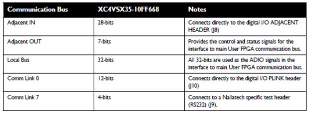
Bus Summary
4.7 CHIP SCOPE
Product description
The LogiCORE Virtual Chip Virtual I / O Core (VIO) is a customizable core that can monitor and boost internal FPGA signals in real time. There are two different types of inputs and two different output types, which are customizable in size to interact with the FPGA design.
Key Features & Benefits
- Provides virtual LEDs and other status indicators via asynchronous and synchronous input ports
- Has input port activity detectors to detect upstream and downstream transitions between samples
- Provides virtual buttons and other controls via asynchronous and synchronous output ports
- For synchronous outputs, it provides the ability to define a pulse train, which is a 16-cycle train of ones and zeros that run at design speed.
The Chip Scope Pro tool inserts the logic analyzer, system analyzer and low-profile virtual I / O software cores directly into its design, allowing you to view any internal signal or node, including hard or soft integrated processors . The signals are captured in the system at the operating speed and drawn through the programming interface, releasing pins for their design. The captured signals are displayed and analyzed using the Chip Scope Pro Analyzer tool.
The Chip Scope Pro tool is also interconnected with its Agilent Technologies bench testing team through the core of the ATC2 software. This core synchronizes the Chip Scope Pro tool with the additional option of the Agilent FPGA dynamic probe. This unique partnership between Xilinx and Agilent delivers deeper trace memory, faster clock speeds, more triggering options and system-level metering capabilities while using fewer pins in the FPGA device.
The Chip Scope Pro serial I / O toolkit provides quick and easy, interactive configuration and debugging of serial I / O channels in high-speed FPGA designs. The Chip Scope Pro serial I / O toolkit allows you to take bit error ratio (BER) measurements on multiple channels and set the high-speed serial transceiver parameters in real time while your serial I / O channels Interact with the rest of the system.
The Chip Scope Pro tool is used to model the XILINX ISE design in the FPGAVirtex6 hardware. The bit stream file generated in XILINX ISE is carried in the Virtex6 FPGA kit. The digital-to-analog converter takes the digital data from Virtex6 FPGA and converts it to analog format and displays it on the oscilloscope. The Chip Scope Pro solution helps minimize the amount of time needed to download and debug. In addition, it is described how the objective RCS influences the performance of radar detection that constitutes the representation of control parameters of RCS.
The FPGA implementation is performed through compile-time and run-time parameters that include the normalization interval, the distance threshold, and the length of the fading cycle that are involved in the logs, which are defined by the user and They can also be changed during runtime. These control parameters create a user-defined environment in which the response obtained from FPGA can be dynamically and dynamically adapted to this environment at compile time at run time. The transmission data obtained from this FPGA solution response is further processed in the host computer.
The implementation of FPGA is of a modular nature in which design consideration can be further modified based on future requirements in FPGA implementations The implementation of FPGA is verified in simulation using XILINX ISE and hardware in an innovative integration Virtex6 .FPGA hardware board running at 200 MHz frequency.
4.7.1 FEATURES OF CHIP SCOPE:
The new RX Margin Analysis tool leverages the Eye Scan function of 7-series FPGA transceivers, allowing our users to interactively characterize and optimize channel quality in real-time and view test results offline.
- Analyze any internal FPGA signal, including built-in processor system buses
- Inserts configurable low-profile software cores during design capture or after synthesis
- All Chip Scope Pro cores are available through the Xilinx CORE Generator ™ system
- Analyzer trigger and capture enhancements make repetitive action easy to do
- Enhancements to the Virtex-5 and Virtex-6 System Monitor console provide access to temperature, voltage, and external sensor data
- Change the probe points without re-implementing the design
- Debug through a network connection through remote debugging, from your office to the lab or around the world
- Integration and generation of Chip Scope cores integrated into Project Navigator and Plan Ahead tool flows
- Add debugging probes directly to HDL (VHDL and Verilog) or restriction files.
4.7.3 Functional Description
The VIO core is a customizable core that can monitor and conduct internal FPGA signals in real time. Unlike the ILA and IBA cores, no non-chip or off-chip RAM is required.
There are four types of signals available in the VIO kernel:
Asynchronous inputs:
These are sampled using the JTAG clock signal that is driven from the JTAG cable. The input values are periodically re-read and displayed on the analyzer.
Synchronous inputs:
These are sampled using the design clock. The input values are periodically re-read and displayed on the analyzer.
Asynchronous Outputs:
These are defined by the user in the analyzer and expelled from the core to the surrounding design. A logic value of 1 or 0 can be defined for individual asynchronous outputs.
Synchronous outputs:
These are defined by the user in the analyzer, synchronized with the design clock and expelled from the core to the surrounding design. A 1 or a logical 0 can be defined for individual synchronous outputs. It is also possible to define pulse trains of 16 clock cycles of ones and zeros for synchronous outputs.
Activity detectors
Each VIO core input has additional cells to capture the presence of transitions in the input. Since the design clock is likely to be much faster than the Analyzer sampling period, it is possible that the signal being monitored will often pass between successive samples. The activity detectors capture this behavior and the results are displayed along with the value in the analyzer.
In the case of a synchronous input, activity cells capable of monitoring synchronous and asynchronous events are used. This feature can detect faults as well as synchronous transitions in the synchronous input signal.
Pulse trains
Each synchronous output VIO has the ability to emit a static 1, a static 0, or a stream of pulses of successive values. A pulse train is a cycle sequence of 16 cycles of 1s and 0s that expel the core in successive design clock cycles. The pulse train sequence is defined in the parser and is executed only once after it is loaded into the kernel.
The VIO core is a customizable core that can monitor and conduct internal FPGA signals
In the case of a synchronous input, activity cells capable of monitoring synchronous and asynchronous events are used. This feature can detect faults as well as synchronous transitions
4.8 DCM MODULE
The primitive Digital Clock Manager (DCM) in Xilinx FPGA parts is used to implement delay loop, digital frequency synthesizer, digital phase shifter or a digital propagation spectrum. The digital clock manager module is a wrapper around the DCM primitive that allows its use in the EDK tool suite.
Characteristics
- Wrap around DCM primitive FPGA architecture; Provides full support for use with EDK design tools.
- Supports both active high and low active reset and configurable BUFG insertion.
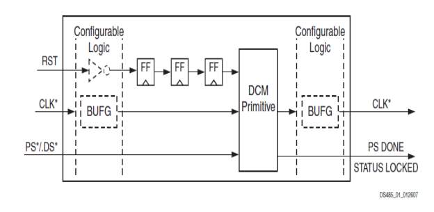
Figure 4.9: DCM Module Block Diagram
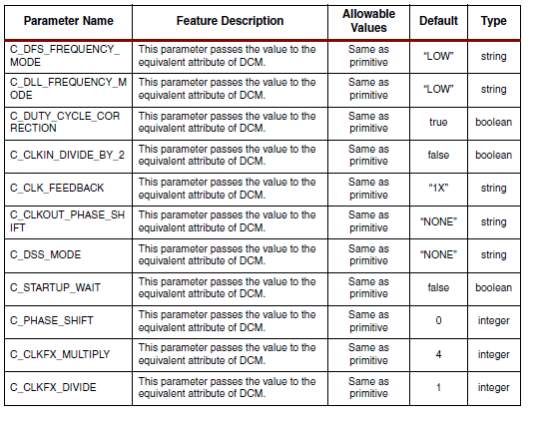
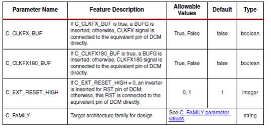
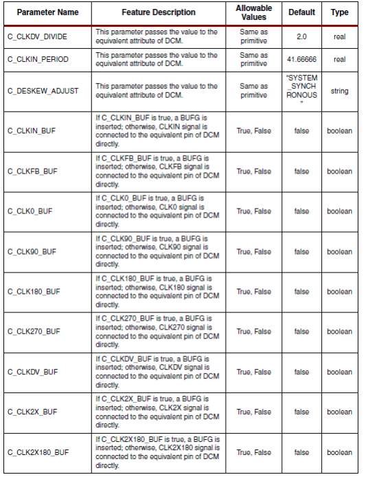
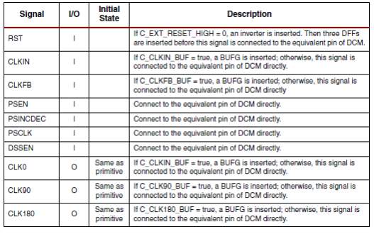
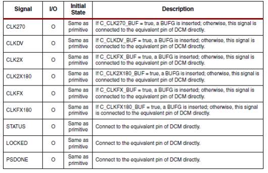
4.8.1 DCM Module Parameters
DCM Module I/O Parameters
Chapter 5 Test Setup And Results
5.1 Block Diagram:

MEMORY REGISTERS


SIGNAL GENERATOR
OUTPUT
ADC
FPGA


CLOCK SIGNAL
5.2 Test Setup:


5.3 Result:
XTREME DSP KIT
Signal Generator
P.C
JTAG
Power Supply

Figure 5.2: Maximum frequency at bin 0
Input Frequency: 1 MHz
Input Voltage: 0.5V
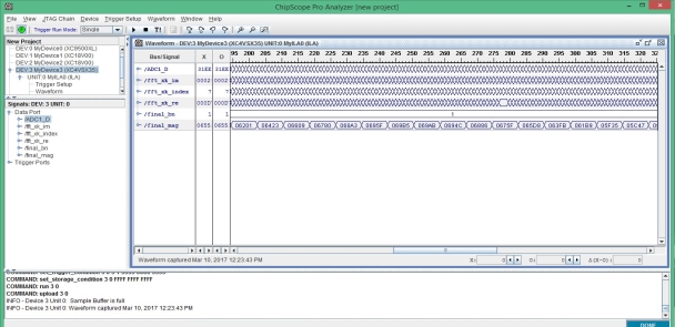
Figure 5.1: Maximum frequency at bin 1
Input Frequency: 13 MHz
Input Voltage: 0.5V
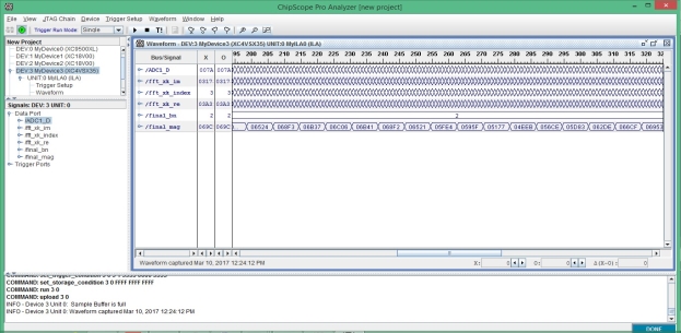
Figure 5.3: Maximum frequency at bin 2
Input Frequency: 26 MHz
Input Voltage: 0.5V
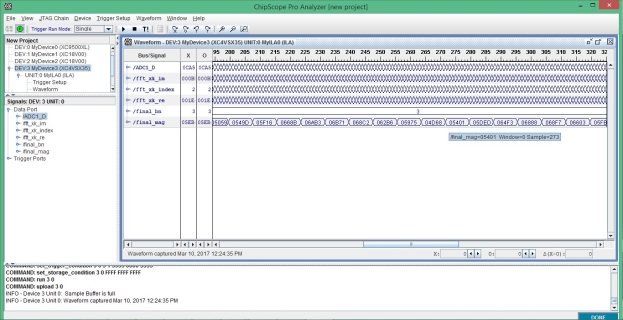
Figure 5.4: Maximum frequency at bin 3
Input Frequency: 39 MHz
Input Voltage: 0.5V
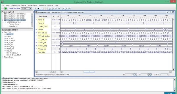
Figure 5.5: Pulse Width of the signal for 8point FFT
T on: 400us
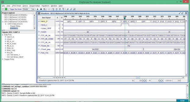
Figure 5.6: Pulse Width of the signal for 256 point FFT
T on: 2us
Chapter 6 Conclusion
6.1. CONCLUSION
The digital receiver based system is the modern day solution for the interception, detection and analysis of basic as well as advanced radars in real time with high parameter accuracies and sensitivity. So with the help of this technique we are able to measure the parameters of an unknown RADAR pulse on the DSP kit. This helps us to take counter measure against the enemy signals.
6.2 APPLICATIONS
Finding the pulse parameters of the unknown received signal has utmost importance in electronic warfare.
The radar esm and ecm systems depends on accurately finding the unknown signal parameters.
This is also useful in generating pulse descriptor words (PDW).
References
1. Pace, P. E. Detecting and classifying LPI radar. Ed. 2nd, Artech House, 2008.
2. James, Tsui. Special design topics in wideband digital receivers. Artech House Inc., Norwood, Massachusetts, 2010.
3. Pekau, H. & Haslett, J.W. A comparison of analog front end architectures for digital receivers. In the Proceedings of the IEEE CCECE/CCGEI, Saskatoon, May 2005.
4. Barkan, Uri & Yehuda, Shuki. Trends in radar and electronic warfare technologies and their influence on the electromagnetic spectrum evolution. In the Proceedings of the IEEE 27th Convention of Electrical and Electronics Engineers, Israel, 2012, pp. 5.
5. Quinn, B.G. Estimating frequency by interpolation using Fourier coefficients. IEEE Trans. Signal Proc., 1994, 42, 12641268.
ANNEXURE
MAIN CODE:
library IEEE;
use IEEE.STD_LOGIC_1164.ALL;
–use IEEE.STD_LOGIC_ARITH.all;
use IEEE.STD_LOGIC_UNSIGNED.all;
— Uncomment the following library declaration if using
— arithmetic functions with Signed or Unsigned values
–use IEEE.NUMERIC_STD.ALL;
— Uncomment the following library declaration if instantiating
–library UNISIM;
–use UNISIM.VComponents.all;
entity toplevel is
port(
— main clock input from oscilator
CLK1_FB : in std_logic;
— adc 14 bit data inputs
ADC1_D      : in  std_logic_vector(13 downto 0);
——————DAC data
CONFIG_DONE : out std_logic;
—for chipscope
fft_xk_index: out std_logic_vector(7 downto 0);
fft_xk_re : out std_logic_vector(22 downto 0);
fft_xk_im : out std_logic_vector(22 downto 0);
fft_mag : out std_logic_vector(23 downto 0);
final_mag: out std_logic_vector(23 downto 0);
final_bn:  out std_logic_vector(7 downto 0);
timer :out std_logic;
frame_no:out std_logic_vector(7 downto 0);
toa_fin:out std_logic_vector(15 downto 0)
);
end toplevel;
architecture Behavioral of toplevel is
COMPONENT fft_8pt
PORT (
clk : IN STD_LOGIC;
ce : IN STD_LOGIC;
start : IN STD_LOGIC;
xn_re : IN STD_LOGIC_VECTOR(13 DOWNTO 0);
xn_im : IN STD_LOGIC_VECTOR(13 DOWNTO 0);
fwd_inv : IN STD_LOGIC;
fwd_inv_we : IN STD_LOGIC;
rfd : OUT STD_LOGIC;
xn_index : OUT STD_LOGIC_VECTOR(7 DOWNTO 0);
busy : OUT STD_LOGIC;
edone : OUT STD_LOGIC;
done : OUT STD_LOGIC;
dv : OUT STD_LOGIC;
xk_index : OUT STD_LOGIC_VECTOR(7 DOWNTO 0);
xk_re : OUT STD_LOGIC_VECTOR(22 DOWNTO 0);
xk_im : OUT STD_LOGIC_VECTOR(22 DOWNTO 0)
);
END COMPONENT;
COMPONENT clock_div
PORT(
CLKIN_IN : IN std_logic;
CLKFX_OUT : OUT std_logic;
CLKIN_IBUFG_OUT : OUT std_logic;
CLK0_OUT : OUT std_logic
);
END COMPONENT;
–signal ADC1_Di: std_logic_vector(13 downto 0);
signal rfd_1,busy_1,edone_1,done_1,dv1,CLK_1,clk_out: std_logic;
signal xn_index_1,xk_index_1,temp1,temp2,temp_index,final_bin,count: std_logic_vector(7 downto 0);
signal xk_re1,xk_im1,xk_repo,xk_impo: std_logic_vector(22 downto 0);
signal mag_o,temp_peak,final_peak_amplitude: std_logic_vector(23 downto 0);
signal free_c,toa_fin_1:std_logic_vector(15 downto 0);
begin
–free_c<=”00000000″;
–count<=”000″;
–toa_fin<= toa_fin_1;
Inst_clock_div: clock_div PORT MAP(
CLKIN_IN => CLK1_FB,
CLKFX_OUT => CLK_1,
CLKIN_IBUFG_OUT => open ,
CLK0_OUT => clk_out   );
freq_trans : fft_8pt
PORT MAP (
clk => CLK_OUT,
ce => ‘1’,
start => ‘1’,
xn_re => ADC1_D,
xn_im => “00000000000000”,
fwd_inv => ‘1’,
fwd_inv_we => ‘1’,
rfd => rfd_1,
xn_index => xn_index_1,
busy => busy_1,
edone => edone_1,
done => done_1,
dv => dv1,
xk_index => xk_index_1,
xk_re => xk_re1,
xk_im => xk_im1
);
conversion : process(dv1,clk_out)
begin
if CLK_OUT’event  and CLK_OUT=’1′ then
fft_xk_index<=xk_index_1;
temp1<=xk_index_1;
if dv1 =’1′ then
if xk_re1(22)=’1′ then
xk_repo <= not(xk_re1)+’1′;
else
xk_repo <= xk_re1;
end if;
if xk_im1(22)=’1′ then
xk_impo <= not(xk_im1)+’1′;
else
xk_impo <= xk_im1;
end if;
fft_xk_re<=xk_repo;
fft_xk_im<=xk_impo;
end if;
end if;
end process;
addition_and_comparision: process(dv1,CLK_OUT)
begin
if CLK_OUT’event  and CLK_OUT=’1′ then
temp2<=temp1;
if dv1=’1′ then
mag_o <= (‘0’ & xk_repo) + (‘0′ & xk_impo);
fft_mag<=mag_o;
end if;
if temp2 <= “11111111” then
if temp2 = “00000000”then
temp_peak<=mag_o;
temp_index<=temp2;
elsif mag_o > temp_peak then
temp_peak<=mag_o;
temp_index<=temp2;
end if;
end if;
end if;
end process;
final_process :process(CLK_OUT)
begin
if CLK_OUT’event  and CLK_OUT=’1′ then
if temp2 = “11111111” then
final_peak_amplitude<=temp_peak;
final_bin<=temp_index;
end if;
final_mag<=final_peak_amplitude;
final_bn<=final_bin;
end if;
end process;
freecounter : process(clk_1)
begin
–free_c<=”0000000″;
if clk_1’event and clk_1=’1′ then
if free_c=”1111111111111111″ then
free_c<=”0000000000000000″;
else
free_c<= free_c +’1′;
end if;
toa_fin <= free_c;
end if;
end process;
width_measurement : process(CLK_OUT)
begin
if CLK_OUT’event  and CLK_OUT=’1′ then
–count <= “000”;
if final_bin > “001” then
if done_1 =’1′ then
count<= count +’1’;
end if;
else
count<= “00000000”;
end if;
end if;
frame_no <= count;
end process;
timer<=clk_1;
——– module configured
CONFIG_DONE <= ‘0’;
end Behavioral;
DCM CODE
library ieee;
use ieee.std_logic_1164.ALL;
use ieee.numeric_std.ALL;
library UNISIM;
use UNISIM.Vcomponents.ALL;
entity clock_div is
port ( CLKIN_IN        : in    std_logic;
CLKFX_OUT       : out   std_logic;
CLKIN_IBUFG_OUT : out   std_logic;
CLK0_OUT        : out   std_logic);
end clock_div;
architecture BEHAVIORAL of clock_div is
signal CLKFB_IN        : std_logic;
signal CLKFX_BUF       : std_logic;
signal CLKIN_IBUFG     : std_logic;
signal CLK0_BUF        : std_logic;
signal GND_BIT         : std_logic;
signal GND_BUS_7       : std_logic_vector (6 downto 0);
signal GND_BUS_16      : std_logic_vector (15 downto 0);
begin
GND_BIT <= ‘0’;
GND_BUS_7(6 downto 0) <= “0000000”;
GND_BUS_16(15 downto 0) <= “0000000000000000”;
CLKIN_IBUFG_OUT <= CLKIN_IBUFG;
CLK0_OUT <= CLKFB_IN;
CLKFX_BUFG_INST : BUFG
port map (I=>CLKFX_BUF,
O=>CLKFX_OUT);
CLKIN_IBUFG_INST : IBUFG
port map (I=>CLKIN_IN,
O=>CLKIN_IBUFG);
CLK0_BUFG_INST : BUFG
port map (I=>CLK0_BUF,
O=>CLKFB_IN);
DCM_ADV_INST : DCM_ADV
generic map( CLK_FEEDBACK => “1X”,
CLKDV_DIVIDE => 2.0,
CLKFX_DIVIDE => 1,
CLKFX_MULTIPLY => 2,
CLKIN_DIVIDE_BY_2 => FALSE,
CLKIN_PERIOD => 9.524,
CLKOUT_PHASE_SHIFT => “NONE”,
DCM_AUTOCALIBRATION => TRUE,
DCM_PERFORMANCE_MODE => “MAX_SPEED”,
DESKEW_ADJUST => “SYSTEM_SYNCHRONOUS”,
DFS_FREQUENCY_MODE => “LOW”,
DLL_FREQUENCY_MODE => “LOW”,
DUTY_CYCLE_CORRECTION => TRUE,
FACTORY_JF => x”F0F0″,
PHASE_SHIFT => 0,
STARTUP_WAIT => FALSE)
port map (CLKFB=>CLKFB_IN,
CLKIN=>CLKIN_IBUFG,
DADDR(6 downto 0)=>GND_BUS_7(6 downto 0),
DCLK=>GND_BIT,
DEN=>GND_BIT,
DI(15 downto 0)=>GND_BUS_16(15 downto 0),
DWE=>GND_BIT,
PSCLK=>GND_BIT,
PSEN=>GND_BIT,
PSINCDEC=>GND_BIT,
RST=>GND_BIT,
CLKDV=>open,
CLKFX=>CLKFX_BUF,
CLKFX180=>open,
CLK0=>CLK0_BUF,
CLK2X=>open,
CLK2X180=>open,
CLK90=>open,
CLK180=>open,
CLK270=>open,
DO=>open,
DRDY=>open,
LOCKED=>open,
PSDONE=>open);
end BEHAVIORAL;
UCF CODE:
#NET “clk1_fb” LOC = B14;
#Control and setup
##NET RESETl LOC =  H3;
NET CONFIG_DONE LOC =  AC1;
#User Status LEDs
#NET LED1_Green LOC =  D3;
#NET LED1_Red LOC =  F3;
#NET LED2_Green LOC =  E26;
#NET LED2_Red LOC =  D26;
#Clock Feedback signals from Clock Driver
NET CLK1_FB PERIOD = 9.5ns;
NET CLK1_FB LOC = B15;

################
## ADC Signals
net adc1_d<*> offset = in 3ns before CLK_OUT;
#net adc2_d<*> offset = in 3ns before CLK1_FB;
#net dac1_d<*> offset = out 4.5ns after CLK1_FB;
#net dac2_d<*> offset = out 4.5ns after CLK1_FB;

#ADC Channel 1
#This is the inner one of the ADCs
NET “adc1_d<0>” LOC = C17; #INTERNAL NOTE: On Schematics signals are ADC2_**
NET “adc1_d<1>” LOC = D19; #they are named as ADC1_** for consistancy with the other versions
NET “adc1_d<2>” LOC = D20;
NET “adc1_d<3>” LOC = C21;
NET “adc1_d<4>” LOC = B18;
NET “adc1_d<5>” LOC = D18;
NET “adc1_d<6>” LOC = C19;
NET “adc1_d<7>” LOC = C20;
NET “adc1_d<8>” LOC = B20;
NET “adc1_d<9>” LOC = B17;
NET “adc1_d<10>” LOC = A17;
NET “adc1_d<11>” LOC = A18;
NET “adc1_d<12>” LOC = A19;
NET “adc1_d<13>” LOC = A20;
#NET “adc1_dry” LOC = D21;
#NET “adc1_ovr” LOC = D17;

################
## DAC Signals
#DAC Channel 1   #This is the DAC at the edge of the board
#NET “dac1_d<1>” LOC = C7; #they are renamed as DAC1_ for consistency with versions
#NET “dac1_d<2>” LOC = B7;
#NET “dac1_d<3>” LOC = C5;
#NET “dac1_d<4>” LOC = D4;
#NET “dac1_d<5>” LOC = C4;
#NET “dac1_d<6>” LOC = A4;
#NET “dac1_d<7>” LOC = B3;
#NET “dac1_d<8>” LOC = B6;
#NET “dac1_d<9>” LOC = E6;
#NET “dac1_d<10>” LOC = D6;
#NET “dac1_d<11>” LOC = A6;
#NET “dac1_d<12>” LOC = A5;
#NET “dac1_d<13>” LOC = B4;
#NET “dac1_div0” LOC = F4;
#NET “dac1_div1” LOC = D5;
#NET “dac1_mod0” LOC = A3;
#NET “dac1_mod1” LOC = E4;
#NET “dac1_plllock” LOC = C6;
#NET “dac1_reset” LOC = E5;
Cite This Work
To export a reference to this article please select a referencing stye below:
Related Services
View all


Related Content
All TagsContent relating to: "Computer Science"
Computer science is the study of computer systems, computing technologies, data, data structures and algorithms. Computer science provides essential skills and knowledge for a wide range of computing and computer-related professions.
Related Articles

DMCA / Removal Request
If you are the original writer of this dissertation and no longer wish to have your work published on the UKDiss.com website then please: