Development of a Monitoring Receiver Based on Digital Signal Processing
Info: 24619 words (98 pages) Dissertation
Published: 16th Dec 2019
Tagged: Computer Science
ABSTRACT
A monitoring receiver plays a very important role in the application of spectrum usage policies, in national security applications and, in fact, in the battlefield for gathering intelligence through the interception of Adversary radio communication links. This project report presents the development of a monitoring receiver based on digital signal processing with the help of various demodulation techniques. The project is limited to Analog demodulation techniques such as Amplitude modulation, Frequency modulation, Double sideband suppressed carrier and Suppressed single side band carrier, design of an appropriate model, simulation verification and finally porting on FPGA.
The design of the VLSI-based system involves the use of existing FPGA (Field Programmable Gate Array) or CPLD (Complex Programmable Logic Device) and its associated tools to create new systems. For modulation and demodulation techniques, we have used Virtex 7 FPGA as a development Platform and Xilinx’s Vivado Design Suite System Generator 2015.1 edition as a development tool. Xilinx Vivado Design Suite 2015.1 edition was used for testing and verification of the design model.
In this project, the monitoring receiver operates in the frequency range of 30 – 1000MHZ (VHF /UHF).When a signal is received, an RF(radio frequency) module converts it to IF (intermediate frequency) of 10.7MHz. This IF is digitized by ADC (analog to digital converter) of the Virtex 7 FPGA card with a sampling frequency of 51.2 MHz
The demodulation algorithms developed for the various analog modulation schemes involve the use of DSP applications such as Digital Down-Convertor (DDC), Digital Up-Convertor (DUC), Filtering and Convolution. The bandwidth for the operation is chosen by the bandwidth selection block. Once the bandwidth and type of signal modulation are chosen, the signal is demodulated. The output of the demodulator is an audio sample from which the original message can be read.
LIST OF FIGURES
Figure 2: General View of Monitoring Receiver
Figure 4: Illustration of a Logic Cell
Figure 5: Software Defined Radio Architecture for Monitoring Receiver
Figure 6: Monitoring Receiver’s Front End
Figure 7: VC707 Evaluation Board
Figure 9: Sine Source Block Parameters
Figure 10: Digital Filter Design Block
Figure 11: Digital Filter Design Parameters
Figure 13: Product Block Parameters
Figure 14: Spectrum Scope Block
Figure 17: System Generator Token
Figure 18: System Generator Parameters
Figure 19: DDS Compiler and its Parameters
Figure 20: FIR Compiler and its Parameters
Figure 21: FDA Tool Parameters
Figure 22: Cordic atan Block Parameters
Figure 27: Amplitude Modulation and Demodulation
Figure 28: Double Side Band Specta of baseband and AM Signals
Figure 29: Power of an AM plotted against frequency
Figure 30: Modulated Depth: Unmodulated carrier has amplitude of 1
Figure 32: Spectrum Plot of a DSB-SC Signal
Figure 33: SSB Modulation and Demodulation
Figure 34: Obtaining I and Q Components
Figure 35: Amplitude Modulation using IQ Components
Figure 36: Frequency Modulation using IQ Components
Figure 37: Mixed Demodulator for FM
Figure 38: AM and FM combined into a single hardware Model
Figure 39: Block Diagram of System Model
Figure 40: DDC: I and Q Components obtained from multiplying received signal with signal from DDS
Figure 42: DDC Filters for multi-stage Down-Sampling
Figure 43: Bandwidth Selection Block
Figure 44: Bandwidth Selection for both I and Q components
Figure 47: Model of Monitoring Receiver
Figure 48: Signal Sources for the Monitoring Receiver
Figure 52: Starting Page for creating a project
Figure 53: Select Virtex 7 VC707 evaluation Board Platform 1.1
Figure 55: Monitoring Receiver IP
Figure 56: LUTs of FPGA used for Monitoring Receiver
Figure 57: Area occupied by monitoring receiver in Sectors of FPGA
Figure 58: Block view of the Project
Figure 59: Sine Wave Output from DDS
Figure 60: Cosine Wave Output from DDS
Figure 62: AM: a) Demodulated wave b) Modulated Wave
Figure 63: FM: a) Demodulated Wave b) Modulated Wave
Figure 64: DSB-SC: a) Demodulated Wave b) Modulated Wave
Figure 65: SSB: a) Demodulated Wave b) Modulated Wave
LIST OF TABLES
Table 1: FPGA Resource Comparison………………………16
Table 2: Virtex-7 XC7VX485T Features……………………19
Table 3: Output of Band………………………………………………………..78
Table 4: Selection Line and MUX Output……………………80
Table of Contents
2. Defence Electronics Research Laboratory
5.2 Field Programmable Gate Arrangement (FPGA)
6.1.1 Software Defined Receiver
6.1.3 Architecture of Monitoring Receiver
6.2.1 Selection of Processing Hardware
.8. Modulation and Demodulation
10. Design Verification Using FPGA
1. Introduction
Communications technology has progressed by leaps and bounds in recent years and has become a part of our daily lives. People communicate through emails, faxes, mobile phones, messaging – texts, audio and video, social media channels. The Internet of Things, 5G mobile technologies etc involves in increasing the use of limited RF spectrum necessitating regulation and control in its use to ensure safety and correct usage.
The ease of access to such advanced technology also poses a major threat when placed in wrong hands. Solutions for ensuring homeland security need to be developed. Security needs to be assured in Hospitals, public places like malls and food joints. New advanced user friendly surveillance and monitoring systems need to be installed at Police Stations, on National Highways, offices and also in the city, while respecting individual privacy.
One of the most critical requirements in security is a monitoring system. Every organization needs a monitoring system be it small or big. In most cases, companies that rely on data networks use software that automatically tests their system and alerts if something is wrong. Many of these software systems can perform data backups and give regular updates on the amount of server space or memory left on the system. On the other hand, larger organizations and those supporting large servers may need a more intensive solution for monitoring purposes.
As the world moves towards hands free wireless solutions that are omnipresent in the form of Bluetooth receivers, mobile 4G and 5G communications, Wi-Fi, Microwave, Satellite communications and so on, the fight to get a share of the limited RF spectrum and development of technologies to make efficient use of available spectrum is occupying technologists and designers all over the world. Monitoring spectrum use by regulatory bodies is therefore of paramount importance.
Electronic warfare has become important facet involving Interception and monitoring of enemy electronic transmissions. Therefore, it is necessary to develop efficient monitoring receivers that can extract intelligence from the multitude of waveforms that prevail on a battlefield.
2. Defence Electronics Research Laboratory
DEFENSE ELECTRONICS RESEARCH LABORATORY is a laboratory of DRDO located in Hyderabad, which actively participates in the design and development of integrated systems of Electronic Warfare for the Armed Forces of India. It was established in 1962 under the aegis of the Defence Research and Development Organization, Ministry of Defence, to meet the current and future needs of the three services – Army, Navy and Air Force equipping them with Electronic Warfare Systems.
DLRL has been entrusted with primary responsibility for the design and development of electronic warfare systems covering both communication and RADAR frequency bands. DLRL consists of a large number of dedicated technical and scientific personnel adequately supported by sophisticated hardware and software development facilities.
DLRL has a number of supporting and technology groups to help the completion of the projects on time and to achieve a quality product. Some of the supporting and technology groups are Printed Circuit Board Group, Antenna Group, Microwave and Millimetre Wave Components Group, Mechanical Engineering Group, LAN, Human Resources Development Group, etc. In addition to the work centres that carry out the design and development activities of the system.
On-site printed circuit board installations provide the fastest realization of digital hardware. Manufacturing facilities of the multilayer Printed Circuit Board are available to meet high precision and denser packaging.
The Antenna Group is responsible for design and development of wide variety of antennas covering a broad electromagnetic spectrum (HF to Millimetre Frequencies). The Group also develops RADOMES, which meet stringent environmental conditions for the EW equipment to suit the platform.
The MMW Group is involved in the design and development of MMW Sub-systems and also various Microwave Components like Solid State Amplifier, Switches, Couplers and Filters using the latest state-of-the–art technology.
The hybrid microwave integrated circuit group provides microwave components and stupendous components made to measure in the microwave frequency region using thin film and thick film technology.
In the Mechanical Engineering Group the required hardware for EW Systems is designed and developed and the major tasks involved include Structural and Thermal Engineering. The Technical Information Centre, the place of knowledge bank is well equipped with maintained libraries, books, journals, processing etc. Latest Technologies in the electronic warfare around the globe are catalogued and easily accessible.
The Techniques Division of ECM wing is one such work centre where design and development of subsystems required for ECM applications are undertaken. ESM Work Centres deal with design and development of Direction Finding Receivers, Rx Proc etc. for various ESM Systems using state-art-of-the technology by employing various techniques to suit the system requirements by end users. All the subsystems are designed and developed using microwave, and processor/DSP based Digital hardware in realizing real time activities in Electronic Warfare.
Most of the work centres are connected through DLRL LAN (Local LAN) for faster information flow and multi point access of information critical to the development activities. Information about TIC, stores and general administration can be downloaded easily.
The Human Resource Division plays a vital role in conducting various CEP courses, organizing service and technical seminars to upgrade the knowledge of scientists in the laboratory.
DLRL has been awarded the ISO 9001: 2008 certification for the Design and Development of an Electronic Quality Assurance System for Defense Services; Use advanced and cost-effective technology to develop reliable electronic warfare systems on time and continually improve quality through the participation of all members.
3. Electronic Warfare
Electronic warfare is defined as the art and science of preserving the use of the electromagnetic spectrum for friendly use while denying its use to the enemy. In military applications, it refers to any action involving the use of electromagnetic spectrum or directed energy to control the spectrum, attack an enemy, or prevent enemy attacks across the spectrum. The purpose of electronic warfare is to deny the opponent the advantage and ensure friendly and unhindered access to the EM spectrum. EW can be applied from the air, sea, land and space through manned and unmanned systems, and can be addressed to communication, radar or other services.
Communication Electronic Warfare (EW) is one of the key elements of the modern battle scenario, protecting one’s own forces from attack; deny information to the enemy and intercepting and disrupting an enemy’s voice communication and data links.
The sub-divisions of Electronic Warfare can be defined as:
- Electronic Warfare Support(ES)
- Electronic Attack(EA)
- Electronic Protection(EP)
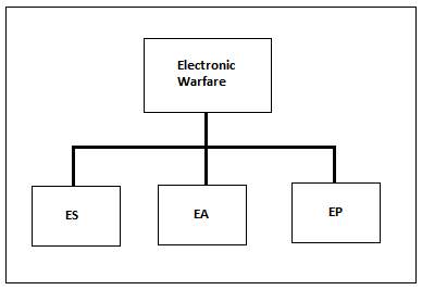
Figure 1: Current NATO electronic warfare definitions divide EW into ES, EA, and EP. EA now includes anti-radiation and directed-energy weapons.[1]
3.1 Electronic Support
Support for electronic warfare is a division of electronic warfare involving actions directed or under the direct control of an operational commander to seek, intercept, identify and locate or locate sources of intentional or unintentional radiated electromagnetic energy for immediate threat purposes Recognition, orientation, planning and realization of future operations. Electronic warfare support systems are a source of information for immediate decisions involving electronic attack, electronic protection, avoidance, targeting, and other tactical uses of forces.
E-war support systems collect data and produce information or intelligence to:
- Corroborate other sources of information or intelligence.
- Conduct direct electronic attack operations.
- Initiate self-protection measures.
- Task of weapons systems.
- Support electronic protection efforts.
- Create or update EW databases.
- Support information tasks.
3.2. Electronic Attack
Electronic attack is a division of electronic warfare involving the use of electromagnetic energy, directed energy or anti-radiation weapons to attack personnel, installations or equipment with the intent to degrade, neutralize or destroy enemy combat capability and is considered a Fire shape
The electronic attack includes:
- Actions taken to prevent or reduce the effective use of the electromagnetic spectrum by the enemy, such as jamming and electromagnetic deception.
- Use of weapons that use electromagnetic or directed energy as their main destructive mechanism (laser, radiofrequency weapons, particle beams).
- Offensive and defensive activities, including countermeasures.
3.3 Electronic Protection
Electronic Protection is a division of electronic warfare involving actions taken to protect personnel, installations and equipment from any friendly or enemy use of the electromagnetic spectrum that degrade, neutralize or destroy friendly combat capability. Electronic protection measures minimize the ability of the enemy to carry out the support of electronic warfare and successful electronic attack operations against friendly forces [2].
To protect friendly combat capabilities, units:
- Regularly report force personnel on the new threat.
- Ensure that electronic system capabilities are protected during exercises, workups, and pre-deployment training.
- Coordinate and deactivate the use of the electromagnetic spectrum.
- Provide training during the planning and training activities of the station of origin on appropriate active and passive electronic protection measures.
- Take appropriate measures to minimize the vulnerability of friendly receivers to enemy jam (such as reduced power, short transmission and directional antennas).
4. Objective
The objective of this project is to develop an Interceptor developed by using various demodulation techniques. Military radio signals operate in a wide range of frequencies and use different modulation techniques necessitating the need for a single intelligent system that can emulate different types of military radio signals. In order to keep up with rapid technological advances in the field of radio communications and overcome early obsolescence, the system must allow incorporation of new coding and demodulation standards through use of programmable processing.
A Software Defined Monitoring Receiver must accrue several benefits for the Military Communications. Interoperability, flexibility, compactness, cost reduction and responsiveness are a few such key benefits. The system architecture of the monitoring receiver should be such that it optimises performance, reliability and cost.
A monitoring receiver is an intercepting receiver. This project finds its relevance in Military applications in a modern battle scenario. The receiver can be used for intercepting and monitoring enemy’s voice communication channel and data links. The intelligence so derived can be further used to gain insight into enemy’s intent and take suitable corrective measures. When used in conjunction with location fixing and electronic attack systems, it lead to derivation of enemy electronic order of battle (EOB) and disruption of his critical communication links.
The main purpose of the monitoring receiver is to continuously check for a signal. The received signal needs to be down converted into a baseband signal for further processing. This can be achieved by using several standardizations that propose to bring the radio frequency to the intermediate frequency. This eases signal processing to a considerable amount. This base-band data would then be routed via various stages of the system so as to retrieve the original message signal. The signal must be filtered, and demodulated according to its bandwidth and mode of operation such that the end result gives the original information that was being carried by the signal.
5. Description
5.1. Monitoring Receiver
Monitoring Receiver forms an important constituent of Electronic Warfare Support (ES). Monitoring is the process of listening to the intelligence in real time by an operator. It operates over a wide range of frequency. It can be single mode as well as multi-mode. Contrary to normal receivers, it is not tuned to a particular frequency or mode; but it detects the signal within a wide frequency band and also detects its mode of operation. Further, upon detection of the type of modulation of the received signal, it demodulates the signal accordingly and extracts information from that. Advanced versions can scan, detect and demodulate multiple signals at the same time.
Figure 2 represents the basic model of a monitoring receiver. This block diagram can be used to explain signal processing in military surveillance systems. The receiver antenna has a radio frequency ranging about 30-1000MHz which is down converted to an intermediate frequency of 10.7MHz.
The main blocks are:
- RF
- ADC
- Evaluation Board.
- Host PC
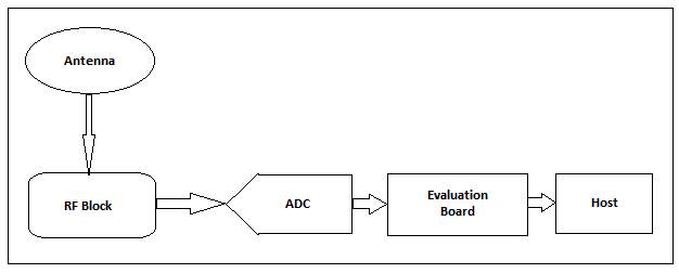
Figure 2: General View of Monitoring Receiver
Radio Frequency Block
The signals received from the antenna are fed to the RF where it undergoes several stages of processing.
ADC
An analog to digital converter (ADC, A / D or A to D) is a device that converts a continuous physical quantity (usually voltage) into a discrete time digital representation of the amplitude of the quantity. An ADC can also provide an isolated measurement. The reverse operation is performed by a digital-to-analog converter (DAC).
Typically, an ADC is an electronic device that converts an input voltage or analog current to a digital number proportional to the magnitude of the voltage or current. However, some non-electronic or only partly electronic devices, such as rotary encoders, may also be considered ADCs. The digital output can use different encoding schemes. Usually the digital output will be a complement two binary number that is proportional to the input, but there are other possibilities.
Evaluation Board
This Evaluation Board is the board which mainly consists of FPGAs where the whole evaluations of the simulation results are dumped with help of generation of the “bit files”. FPGA is the heart of the evaluation board.
Host PC
The result at the end of evaluation will be having either audio or data. If it is audio it is available at speaker and if it is data it is stored in the hard disk. The following are required specifications of PC:
- Processor: Upgraded versions.
- Memory: 4 to 8 GB RAM.
- Hard Disk: 320 GB
- Add on Cards: Xilinx Extreme DSP Development card.
5.2 Field Programmable Gate Arrangement (FPGA)
A field programmable gate array (FPGA) is an integrated circuit that is designed to be configured after manufacture. It is a prefabricated silicon device that can be programmed electrically to become almost any type of circuit or digital system. The FPGA configuration is generally specified using a hardware description language (HDL), similar to that used for an application-specific integrated circuit (ASIC). A software CAD flow transforms a hardware application into a sequence of programming bits, which can be programmed easily and instantly into an FPGA. FPGAs can be used to implement any logical functions that an ASIC could perform.
They provide a number of compelling advantages over fixed-function specific application (ASIC) chip technologies such as standard cells: ASICs take months to manufacture and can cost more than a lakh dollars to get the first device; FPGAs are configured in a few seconds or less and cost from a few dollars to a few thousand dollars. The flexible nature of an FPGA has a significant cost in area, delay and power consumption: an FPGA requires approximately 20 to 35 times more area than a standard cell ASIC, has a speed performance approximately 3 to 4 times Less than one ASIC and consume approximately 10 times more dynamic power. These disadvantages arise in large part from the programmable routing fabric of an FPGA that negotiates area, speed and power in exchange for an “instant” fabrication.
Despite these disadvantages, FPGAs present attractive alternatives for the implementation of the digital system. The re-programmability of an FPGA allows us to run several hardware applications at mutually exclusive times. Likewise, any errors in the final product can be corrected / updated by a simple reprogramming of the FPGA. An FPGA also allows a partial re-configuration, ie only one portion of an FPGA is configured while other portions are still functioning. Compared to alternative technologies that make specific circuits for silicon applications, FPGA-based applications have less non-recurring engineering cost (NRE) and less time to market. These advantages make FPGA-based products very effective and economical for many applications.
5.2.1 FPGA Architecture
FPGAs contain programmable logic components called “logic blocks”, and a hierarchy of reconfigurable interconnects that allow the blocks to be “wired together” somewhat like many logic gates that can be inter-wired in different configurations. Logic blocks can be configured to perform complex combinational functions, or merely simple logic gates like AND, XOR. In most FPGAs, the logic blocks also include memory elements, which may be simple flip-flops or more complete blocks of memory.
What logic functions are performed by the blocks, and how the wires are connected to the blocks and to each-other, can be thought of as being controlled by electronic switches. The settings of these switches are determined by the contents of digital memory cells. For example, if a block could perform any one of the Boolean functions of two inputs, then four bits of this “configuration memory” would be needed to determine its behaviour. The blocks around the periphery of the array have special configuration switches to control how they are interfaced to the external connections of the chip (its pins). An FPGA includes a programmable interconnect structure in which the interconnect resources are divided into two groups. A first subset of the interconnect resources are optimized for high speed. A second subset of the interconnect resources are optimized for low power consumption. In some embodiments, the transistors of the first and second subsets have different threshold voltages. Transistors in the first subset have a lower threshold voltage than transistors in the second subset. The difference in threshold voltages can be accomplished by using different doping levels, wells biased to different voltage levels, or using other well-known means.
The flexibility and reuse of an FPGA is due to its programmable logic blocks that are interconnected through configurable routing resources. An application design can be easily mapped to these configurable resources by using a dedicated software flow. This application is initially synthesized in interconnected logical blocks (usually composed of search tables and flip-flops). The logical block instances of the synthesized circuit are then placed in configurable logic blocks of FPGA. Placement is performed in such a way that minimal routing resources are required to interconnect them.
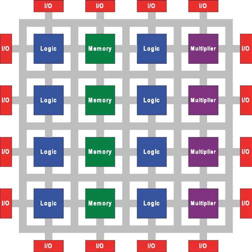
Figure 3: FPGA Architecture[3]
Connections between these logical blocks are later routed using configurable routing resources. Logical blocks and routing resources are programmed by static RAM (SRAMs) that are distributed through the FPGA. Once an application circuit is placed and routed in the FPGA, the SRAM bit information of the entire FPGA is assembled to form a bit stream. This bit-stream is programmed into the FPGA SRAMs by a bit stream loader, which is integrated into the FPGA.
This work focuses only on devices based on SRAM FPGA, since they are the most commonly used commercial FPGAs. Other technologies used to implement memory configuration include anti-fuses and floating gate transistors. An FPGA device can be compared to other digital computing devices.
In addition to digital functions, some FPGAs have analog features. The most common analog feature is the programmable rotation speed and drive force at each output pin, allowing the engineer to set slow speeds on slightly charged pins that would otherwise sound unacceptably and set speeds stronger and faster On pins loaded into high-speed channels that would otherwise run too slow. Another relatively common analog feature is the differential comparators on the input pins designed to be connected to differential signalling channels. A few “mixed signal FPGAs” have peripheral to analog-to-digital (ADC) converters and digital-to-analog converters (DACs) with analog signal conditioning blocks that allow them to function as a system on a chip. Such devices erase the line between an FPGA, which carries digital zeros and zeros in its internal programmable interconnect fabric, and a Field Programmable Analog Array (FPAA), which carries analog values in its internal programmable interconnect fabric.
Modern FPGA families expand on previous capabilities to include higher-level functions fixed on silicon. Having these common functions embedded in the silicon reduces the required area and gives those functions a greater speed compared to the construction of primitives. Examples of these include multipliers, generic DSP blocks, embedded processors, high speed IO logic and embedded memories.
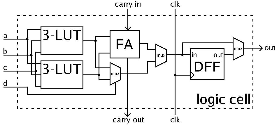
Figure 4: Illustration of a Logic Cell[4]
FPGAs are also widely used for systems validation including pre-silicon validation, post-silicon validation, and firmware development. This allows chip companies to validate their design before the chip is produced in the factory, reducing the time-to-market.
5.2.2 FPGA Families
FPGA is classified into different types:
- Kintex
The Kintex-7 family is Xilinx’s first mid-range FPGA family that the company claims offers high performance at low cost while consuming less power. The Kintex family includes a low-cost optimized 6.5 Gbit / s serial connectivity of 12.5 Gbit / s required for applications such as high-volume 10G optical cable communication equipment and provides a balance of processing throughput Signal, power consumption and cost to support the deployment of LTE (Long Term Evolution) wireless networks. - Artix
The Artix-7 family is based on the unified architecture of the Virtex series. Xilinx claims that the Artix-7 FPGAs provide the performance required to address the cost-sensitive high volume markets previously served by low-cost ASSPs, ASICs and FPGAs. The Artix family is designed to address the small form factor and low power performance requirements of portable ultrasonic portable equipment, commercial control of digital camera lenses, and avionics and military communications equipment. Virtex - The Virtex series of FPGAs have integrated features that include FIFO and ECC logic, DSP blocks, PCI-Express controllers, Ethernet MAC blocks, and high-speed transceivers. In addition to FPGA logic, the Virtex series includes embedded fixed function hardware for commonly used functions such as multipliers, memories, serial transceivers and microprocessor cores. These capabilities are used in applications such as wired and wireless infrastructure equipment, advanced medical equipment, test and measurement, DSP applications, and defence systems.
- Zina
the Zynq-7000 family of SoCs addresses high-end embedded-system applications, such as video surveillance, automotive-driver assistance, next-generation wireless, and factory automation. Zynq-7000 integrate a complete Cortex-A9-processor-based 28 nm system. The Zina architecture differs from previous marriages of programmable logic and embedded processors by moving from an FPGA-centric platform to a processor-centric model. For software developers, Zynq-7000 appear the same as a standard, fully featured ARM processor-based system-on-chip (SOC), booting immediately at power-up and capable of running a variety of operating systems independently of the programmable logic. - Spartan
The Spartan series targets applications with a low-power footprint, extreme cost sensitivity and high-volume; e.g. displays, set-top boxes, wireless routers and other applications. The Spartan-6 family is built on a 45-nanometer, 9-metal layer dual-oxide process technology. The Spartan-6 was marketed in 2009 as a low-cost solution for automotive, wireless communications, flat-panel display and video surveillance applications. Mainly used for applications requiring a large number of input and output lines.
From the above FPGA’s Virtex series of the FPGA is the best suited to our application as it is constrained to the features suited for the application.
5.2.3 Virtex
The Virtex series is the flagship family of FPGA products developed by Xilinx. They have built-in features including FIFO and ECC logic, DSP blocks, PCI-Express controllers, MAC Ethernet blocks and high-speed transceivers. In addition to FPGA logic, These are used in applications such as wired and wireless infrastructure equipment, advanced medical equipment, test and measurement and defence systems. Some members of the Virtex family are available in radiation hardened packages, specifically to operate in space where noxious high-energy particle currents can wreak havoc on semiconductors.
Table 1 compares the available resources in the five Xilinx FPGA families:
- Virtex-II Pro: VP
- Virtex-4: FX, LX and SX
- Virtex-5: LX and SX
- Virtex-6: LX and SX
- Virtex-7: VX
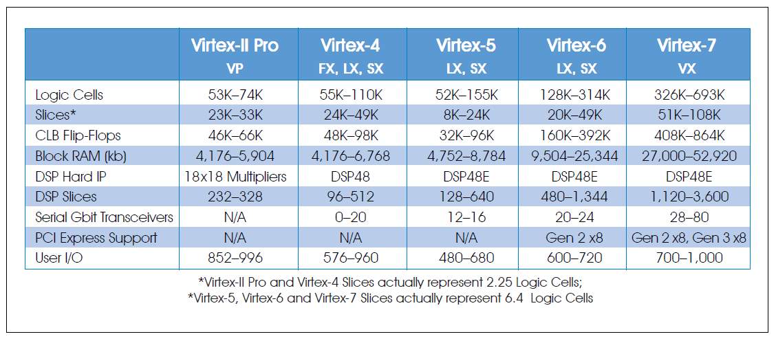
Table 1: FPGA Resource Comparison[5]
The Virtex-II family includes hardware multipliers that support digital filters, meters, demodulators and FFTs, a major benefit for processing software radio signals. The Virtex-II Pro family drastically increased the number of hardware multipliers and also added built-in PowerPC microcontrollers.
The Virtex-4 family is offered as three subfamilies that drastically increase clock speeds and reduce energy dissipation over previous generations. It greatly increases the capabilities of programmable logic design, which is a powerful alternative to ASIC technology. The wide range of Virtex-4 FPGA hard-core IP blocks include Power PC processors (with a new APU interface), three-way Ethernet MAC, 6 Gbit / s 6.5 Gbps serial transceivers, dedicated DSP segments, High-speed management circuits and source synchronous interface blocks.
The Virtex-4 LX family offers maximum logic and I / O pins while the SX family boasts 512 DSP cuts for maximum DSP performance. The FX family is a generous mix of all resources and is the only family that offers RocketIO, PowerPC cores and newly added Gigabit Ethernet ports.
Virtex-5 family of LX devices offer maximum logical resources, gigabit serial transceivers, and Ethernet media access controllers and are designed for mission-critical applications. The SX devices boost DSP capabilities with all the same extras as the LX. Virtex-5 devices offer lower power dissipation, faster clock speeds and improved logic breaks. They also improve synchronization functions to handle faster memory and gigabit interfaces. They support faster dual-end parallel and differential I / O buses to handle faster peripheral devices. With the Virtex-5, Xilinx switched the logical fabric from four LUTs to six LUTs. The Virtex-5 series is a 65 nm design made of 1.0 V triple-oxide process technology.
The Virtex-6 and Virtex-7 devices offer even greater density, more processing power, lower power consumption and updated interface functions to fit the latest technology I / O requirements, including PCI Express. Virtex-6 supports PCIe 2.0 and Virtex-7 supports PCIe 3.0. Large slices of DSP are responsible for most of the processing power of the Virtex-6 and Virtex-7 families. Increases in the operating speed of 500 MHz in V-4, at 550 MHz in V-5, at 600 MHz in V-6, at 900 MHz in V-7 and the continuous increase density allow more slices of DSP for Be included in the same-size package. As shown in Table 1, Virtex-6 outperforms in an impressive 1,344 DSP slices, while Virtex-7 tops out on an even more impressive 3,600 DSP slices. The Virtex-6 family is built on a 40nm process for electronic computing intensive systems, and the company claims that it consumes 15 percent less power and has an improved performance of 15 percent compared to the 40 nm FPGAs that Compete The Virtex-7 2000T FPGA exceeds Moore’s law – Intel’s co-founder Gordon Moore’s prediction that the number of those transistors will double approximately every two years – providing double the number of transistors in a single FPGA that would be expected under prediction. In comparison, Intel’s largest chips have about 2.6 billion transistors.
5.3.4 Series FPGAs Overview
FPGAs in the Xilinx 7 series comprise three new FPGA families that address the full range of system requirements, from low-cost applications, small form factor, cost-sensitive applications and high volume to connectivity bandwidth High-end, logical capability and signal processing capability for the most demanding high-performance applications. The 7 FPGAs in the series include:
- Artix-7 Family: Optimized for lowest cost and power with small form-factor packaging for the highest volume applications.
- Kintex®-7 Family: Optimized for best price-performance with a 2X improvement compared to previous generation, enabling a new class of FPGAs.
- Virtex®-7 Family: Optimized for highest system performance and capacity with a 2X improvement in system performance. Highest capability devices enabled by stacked silicon interconnect (SSI) technology.
Built on high-power, high-performance, low-power (HPL) HKMG 28 nm high-power process technology, the 7-series FPGA enables unprecedented system performance with 2.9 Tb / S I / O bandwidth, 2 million logical cell capacity and 5.3 TMAC / s DSP, while consuming 50% less power than previous generation devices to offer a fully programmable alternative to ASSPs and ASICs.
We have used Virtex 7 XC7VX485T FPGA in the project. The summary of its features is listed below:
| Logic Cells | 485,760 |
| Configurable Logic Blocks (CLLs) – Slices | 75,900 |
| CLLs – Max Distributed Ram (Kb) | 8,175 |
| DSP Slices | 2,800 |
| Block RAM Blocks – 18 Kb | 2,060 |
| Block RAM Blocks – 36 Kb | 1,030 |
| Block RAM Blocks – Max (Kb) | 37,080 |
| CMTs | 14 |
| PCle | 4 |
| GTX | 56 |
| GTH | 0 |
| GTZ | 0 |
| XADC Blocks | 1 |
| Total I/O banks | 14 |
| Max User I/Os | 700 |
| SLRs | N/A |
Table 2: Virtex-7 XC7VX485T Features
Notes:
- Each DSP slice contains a pre-adder, a 25 x 18 multiplier, an adder, and an accumulator.
- Block RAMs are fundamentally 36 Kb in size; each block can also be used as two independent 18 Kb blocks.
- Each CMT contains one MMCM and one PLL.
- Virtex-7 T FPGA Interface Blocks for PCI Express support up to x8 Gen 2. Virtex-7 XT and Virtex-7 HT Interface Blocks for PCI Express support up to x8 Gen 3, with the exception of the XC7VX485T device, which supports x8 Gen 2.
- Does not include configuration Bank 0.
- This number does not include GTX, GTH, or GTZ transceivers.
6. Literature Survey
There has been exponential growth in the means of communication used by people. In recent times exchange of data, audio and video messages has become an inevitable part of our daily lives. Broadcast messaging, command and control communications, emergency response communications are a few examples of communication required in everyday life. Therefore, modifying radios in a cost effective manner has become business critical. Software Defined Radio technology brings the flexibility, cost efficiency and power to drive communications forward with far reaching benefits.
With the increasing computing power of modern microprocessors it becomes feasible to process radio signals completely in software reducing the complexity of the hardware. Using embedded microprocessors in an FPGA and combining them with other advanced features of the fabric allows for a powerful solution on a single, re-programmable chip.
Radio has been always fascinating human beings since its discovery and invention. It provides information and entertainment to the people anywhere at low cost. The analog technologies and the advanced computer systems emphasized and started shifting from hardware to software implementation of systems.
Digital signal processing (DSP) playing a very revolutionary role in the design and implementation of many practical systems with incorporation of the software. DSP can carry out variety of functions using same hardware. Today the DSP’s are available and operated at very high speed at intermediate and radio frequencies. The introduction of software into the radio systems has brought the concept of software radio. Software radios have brought a revolution in the radio engineering. It is now possible to define various radio functions using suitable software on the same hardware. Such radios are referred to as Software Defined Radio (SDR).
The literature survey included the study of the system architecture of a Software Defined Receiver Radio which is running on embedded Linux in a Single FPGA. Further the study gathered advantages of Software Defined Radio on reconfigurable computing systems over existing solutions, whose result is a working SDR application.
6.1 Part I
6.1.1 Software Defined Receiver
Software defined Radio (SDR) is an emerging technology that is profoundly changing the radio system engineering. A Software Defined Radio is a transceiver that can be programmed through software as per the requirement of the application. It consists of functional blocks similar to other digital communication systems. However, the software defined radio receiver concept lays new demands on the architecture in order to be able to provide multi-band, multi-mode operation and re-configurability, which are needed for supporting a configurable set of air interface standards.
6.1.2 Monitoring Receiver
A Monitoring receiver is the radio which continuously checks for transmitted signals, demodulates them upon reception to obtain the original message signal. In this project we combine the advantages of Software Defined Radio and Monitoring Receiver to build a receiver system that senses signals continuously to demodulate them and is software upgradable for future demodulation techniques.
Over the last few years, analog radio systems are being widely used for various radio applications in military, civilian and commercial spaces. Software Defined Monitoring Receiver technology aims to take advantage of programmable hardware modules to build an open architecture based radio system software..
A monitoring receiver system built using SDR technology extends the utility of the system for a wide range of applications that use different link-layer protocols and modulation or demodulation techniques.
SDR technology supports over-the-air upload of software modules to subscriber handsets. Network operators can perform mass customizations on subscriber’s handsets by just uploading appropriate software modules resulting in faster deployment of new services.
Manufacturers can perform remote diagnostics and provide defect fixes by just uploading a newer version of the software module to consumers’ handsets as well as network infrastructure equipment.
The main aim is to develop a model of Software Defined Monitoring Receiver. It is a radio communications receiver system in which all the typical components of a communication system such as mixers, modulators, demodulators, detectors; which are implemented through software programming.
Key Features of SDR Technology:
- Re-configurability
SDR allows co-existence of multiple software modules implementing different standards on the same system allowing dynamic configuration of the system by selecting the appropriate software module to run - Ubiquitous Connectivity
SDR enables implementation of air interface standards as software modules and multiple instances of such modules that implement different standards can co-exist in equipment and handsets - Interoperability
SDR facilitates implementation of open architecture radio systems. End-users can seamlessly use innovative third-party applications on their handsets as in a PC system. This enhances the appeal and utility of the handsets - Multi-Band and Multi-Mode operation
SDR allows a single radio to be operated over wide band of frequencies in different modes based on the type of application
6.1.3 Architecture of Monitoring Receiver
A Monitoring Receiver consists of basic functional blocks of any digital communication system. Functions of a typical digital communication system can be divided into three main functional blocks:
- RF Section
- IF Section
- Base-band Section
RF Section
The RF section also called RF front end consists of essentially analog hardware modules. It is responsible for transmitting/receiving the radio frequency (RF) signal from the antenna via a coupler and converting it to a lower center frequency such that the new frequency range is compatible with the ADC. It also filters out noise and undesired channels and amplifies the signal to the level suitable for the ADC. On the transmit path, RF front-end performs analog up conversion and RF power amplification.
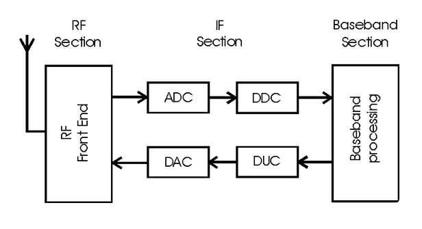
Figure 5: Software Defined Radio Architecture for Monitoring Receiver[6]
IF Section
The IF section contains ADC/DAC and DDC/DUC for increasing bandwidth and matching sampling rates with the previous blocks, which are explained below:
Analog-to-Digital Convertor (ADC)
The ADC blocks perform analog-to-digital conversion (on receive path). ADC blocks interface between the analog and digital sections of the radio system. DAC performs the opposite function of it i.e. digital-to-analog conversion.
Digital Down-Convertor (DDC)
The DDC/DUC and base band processing operations require large computing power and these modules are generally implemented using ASICs or stock DSPs. Implementation of the digital sections using ASICs results in fixed-function digital radio systems. If DSPs are used for base band processing, a programmable digital radio (PDR) system can be realized. In other words, in a software based receiver system base band operations and link layer protocols are implemented in software. The DDC functionality in a SDR system is implemented using ASICs. The limitation of this system is that any change made to the RF section of the system will impact the DDC operations and will require non-trivial changes to be made in DDC ASICs.
Base Band Processing
Digital processing is the key part of any software defined radio. It enables the radio to re-configure to any air interface. The baseband section performs base band operations such as connection setup, equalization, frequency hopping, timing recovery, and correlation and also implements the various demodulation schemes. The front end design of the monitoring receiver is as below.
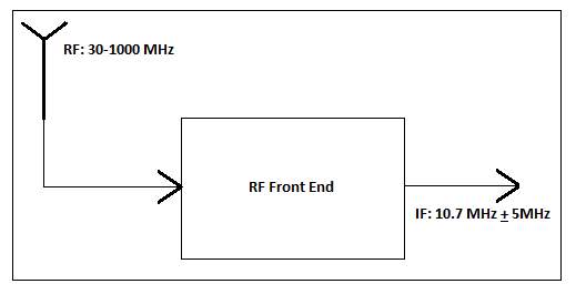
Figure 6: Monitoring Receiver’s Front End
Advantages
- Programmability
- Easy implementation of Radio Functions
- Common hardware for various modulation techniques with ability to transmit and receive
- Re-configurability
- Helps recognize and avoid interference with other communication channels
- Elimination of analog hardware and its cost, resulting in simplification of radio architectures and improved performance; and the chance for new experimentation.
Disadvantages
- Writing software for various target systems is a painstaking task
- The need for interfaces to digital signals and algorithms
- Poor dynamic range in some SDR designs
- A lack of understanding among designers as to what is required
6.2 Part II
6.2.1 Selection of Processing Hardware
The need for re-configurability necessitates the use of programmable digital processing hardware. The reconfiguration may be done at several levels. There may be parameterized components that are fixed ASICs, and in the other end, the hardware itself may be totally reconfigurable, e.g. FPGAs. Customized FPGAs, called configurable computing machines (CCMs), provide real-time paging of algorithms.
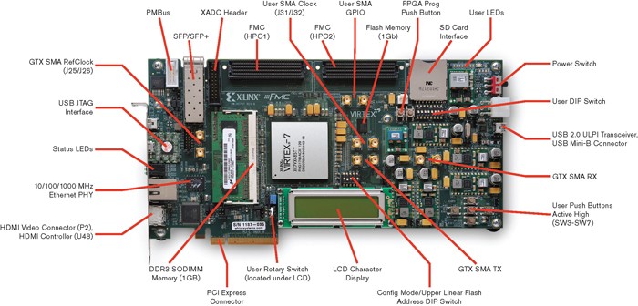
Figure 7: VC707 Evaluation Board[7]
6.2.2 Dynamic Range
Dynamic range is the ratio of the largest tolerable signal to the smallest usable signal[8]. Receiver dynamic range is a central issue for Software Defined Radio (SDR) designers today and a major obstacle to advancement in digital receiver designs. The challenge is to find an effective digital signal processing (DSP) implementation of receiver functions that achieves dynamic range sufficient for the frequency range of interest, which may be VHF, UHF or above.
The dynamic ranges of the current crop of DSP monitoring receivers are determined partly by their analog stages. The idea is to remove such barriers so that performance is extended by analog technology. DSP tends to minimize cost and maximize flexibility in receivers. Data-conversion hardware capabilities have advanced to the point where direct digital conversion (DDC) radios are performing at levels equal to or better than their analog counterparts, provided that an analog filter restricts the bandwidth, to keep the peak voltage in the range of the A/D converter.
The proposed system offers an excellent opportunity to examine new and better ways of defining and measuring dynamic range. Traditional definitions of nonlinear effects in analog circuits, such as intercept point (IP), tend to lose their meaning when applied to digital circuits.
7. Tools Used and Hardware
7.1 MATLAB Simulink Software
MATLAB (Matrix Laboratory) is a numerical computing environment and fourth generation programming language. MATLAB allows manipulation of arrays, tracing of functions and data, implementation of algorithms, creation of user interfaces and interconnection with programs written in other languages, including C, C ++ and FORTRAN. An optional toolbox allows access to symbolic computing capabilities. An additional package, Simulink, adds multi-domain graphical simulation and model-based design for dynamic and integrated systems. MATLAB is widely used in academic and research institutions of engineering, science and economics, as well as industrial enterprises.
MATLAB Simulink
It is a block diagram environment for multi-domain simulation and Model-Based Design. It supports simulation, automatic code generation, and continuous test and verification of embedded systems. Simulink also provides a graphical editor, customizable block libraries, and solvers for modelling and simulating dynamic systems. It is integrated with MATLAB, enabling us to incorporate MATLAB algorithms into models and export simulation results to MATLAB for further analysis.
History
MATLAB was created in the late 1970s by Cleve Moler, the chairman of the computer system department at the University of Mexico. He designed it to give access to his LINPACK and EISPACK without having to learn FORTRAN. Jack Little, who was an engineer joined Moler and Steve Bangert, as he acknowledged his potential after being exposed to it. They rewrote MATLAB in C and founded Math Works in 1984 to continue its development. The rewritten libraries of MATLAB in C were known as JACKPAC. MATLAB 8.4 R2014b presents a new MATLAB graphics system.
A Few Blocks that were used in the project along with their descriptions are given below:
Sine Wave
The Sine wave block provides a sinusoid. The block can operate in time-based or sample-based mode. It is used as input signal to the respective operation:
- Time Based Mode: The output of the Sine Wave block is determined by Time-based mode has two sub modes. They are continuous and discrete modes.
- Using the Sine Wave Block in Continuous Mode: A Sample time parameter value of 0 causes the block to operate in continuous mode. When operating in continuous mode, the Sine Wave block can become inaccurate due to loss of precision as time becomes very large.
- Using the Sine Wave Block in Discrete Mode: If Sample time parameter value greater than zero causes the block to behave as if it were driving a Zero-Order Hold block whose sample time is set to that value.
- Sample-Based Mode: To compute the output of the Sine Wave block.

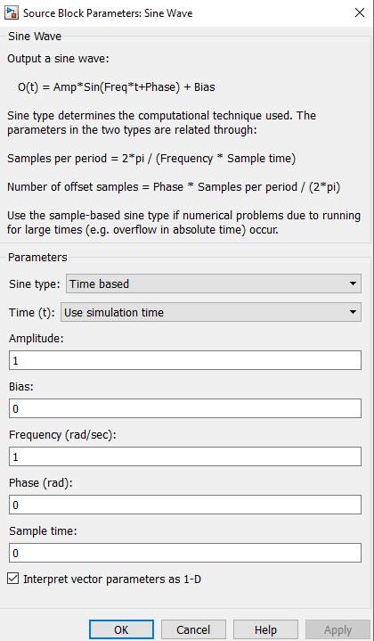
Figure 9: Sine Source Block Parameters
- A is the amplitude of the sine wave.
- p is the number of time samples per sine wave period.
- k is a repeating integer value that ranges from 0 to p–1.
- 0 is the offset (phase shift) of the signal
Filters
In signal processing, a filteris a device or process that removes some frequencies in order to suppress interfering signals and reduce background noise. Correlations can be removed for certain frequency components and not for others without having to act in the frequency domain.
Filters may be:
- linear or non-linear
- passive or active type of continuous-time filter
- Time-invariant or time-variant, also known as shift invariance.
- Chebyshev filter and Butterworth filter
- Infinite impulse response (IIR) or finite impulse response (FIR) type of discrete-time or digital filter.
The frequency response can be classified into a number of different band forms describing which frequency bands the filter passes (the pass band) and which it rejects (the stop band):
- Low-pass filter – low frequencies are passed, high frequencies are attenuated.
- High-pass filter – high frequencies are passed, low frequencies are attenuated.
- Band-pass filters – only frequencies in a frequency band are passed.
- Band-stop filter or band-reject filter – only frequencies in a frequency band are attenuated.
- Notch filter – rejects just one specific frequency – an extreme band-stop filter.
- All-pass filter – all frequencies are passed, but the phase of the output is modified.
Band pass filter is the filter which passes only the required range of frequencies of the signal when it is passed through it. The sampling frequency Fs that you specify in the FDA Tool GUI should be identical to the sampling frequency of the Digital Filter Design block’s input block. When the sampling frequencies of these blocks do not match, the Digital Filter Design block returns a warning message and inherits the sampling frequency of the input block
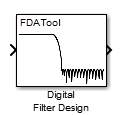
Figure 10: Digital Filter Design Block
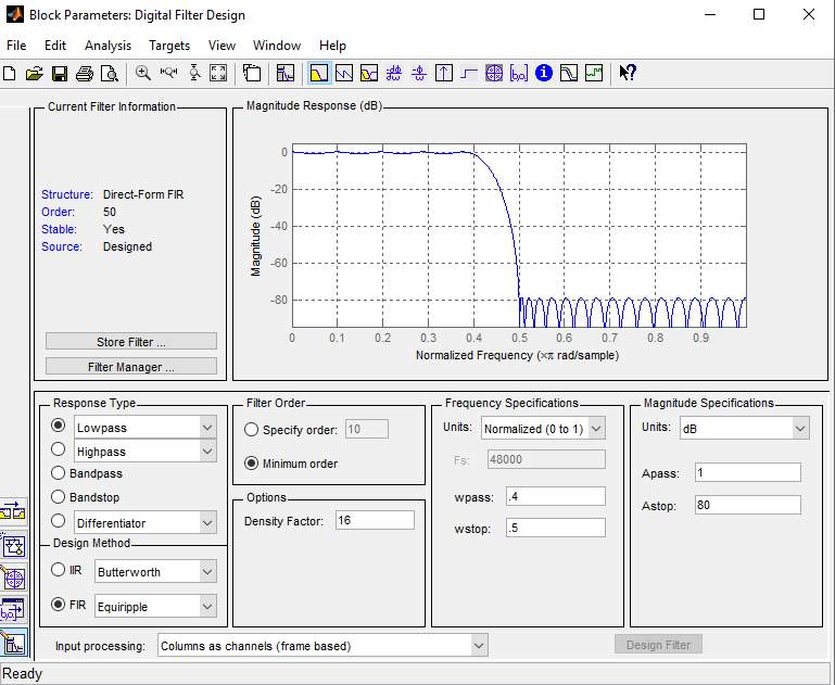
Figure 11: Digital Filter Design Parameters
Product
This block mainly specifies multiply and divides scalars and non-scalars or multiplies and inverts matrices. By default, the Product block outputs the result of multiplying two inputs: two scalars, a scalar and a non-scalar, or two non-scalars that have the same dimensions.
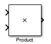
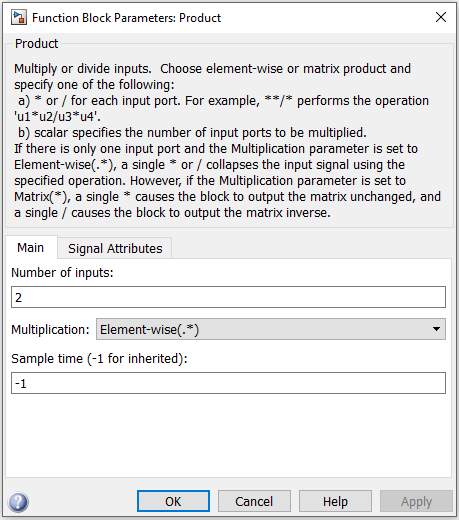
Figure 13: Product Block Parameters
The default parameter values that specify this behaviour are:
Multiplication: Element-wise (.*) No. of inputs=2
Spectrum Scope
The main function of this Spectrum scope is to compute and display period gram of each input signal. The input can be a sample-based or frame-based vector or a frame-based matrix.
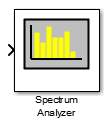
Figure 14: Spectrum Scope Block
The Spectrum unit’s parameter allows specifying the following information:
The type of measurement for the block to compute is Power Spectral Density or Mean-Square Spectrum. The block uses linear or log type of scaling.
Scope
It is used to Display signals generated during simulation. The Scope block displays its input with respect to simulation time. The Scope block can have multiple axes (one per port) and all axes have a common time range with independent y-axes. If you open a Scope after a simulation, the Scope’s input signal or signals will be displayed. If the signal is continuous, the Scope produces a point-to-point plot. If the signal is discrete, the Scope produces a stair-step plot.
Constant
It generates real or complex constant value like scalar, vector, and matrix. Output depends on dimensions of constant value and setting of interpret vector parameter as 1-D parameter. It generates either sample based or frame based, depending on sampling mode parameter. Output of the block has same dimensions and elements as constant value parameter. It outputs a signal whose data type and complexity are same as constant value parameters.

7.2 Xilinx System Generator
The System Generator block provides control of system and simulation parameters, and is used to invoke the code generator. System Generator for DSP is the industry’s leading high-level tool for designing high-performance DSP systems using Xilinx All Programmable devices.
The System Generator block is also referred as ‘token’ because of its unique role in the designing of models. Every Simulink model containing any element from the Xilinx Block-set must contain at least one System Generator block (token).
Compilation:Specifies the type of compilation result that should be produced when the code generator is invoked.
Part:Defines the FPGA part to be used.
Target directory:Defines where System Generator should write compilation results. System Generator and the FPGA physical design tools typically create many files, it is best to create a separate target directory, i.e., a directory other than the directory containing your Simulink.

Figure 17: System Generator Token
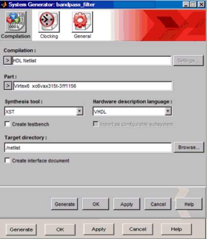
Figure 18: System Generator Parameters[9]
Create Test bench:This instructs System Generator to create a HDL test bench. Simulating the test bench in an HDL simulator compares Simulink simulation results with ones obtained from the compiled version of the design. To construct test vectors, System Generator simulates the design in Simulink, and saves the values seen at gateways. The top HDL file for the testbench is named <name>_testbench.vhd/.v, where <name> is a name derived from the portion of the design being tested.
Clock pin location:It defines the pin location for the hardware clock. This information is passed to the Xilinx implementation tools through a constraints file but not necessary if the System Generator design is to be included as part of a larger HDL design.
FPGA clock period (ns):It defines the period in nanoseconds of the system clock. The value need not be an integer. The period is passed to the Xilinx implementation tools through a constraints file, where it is used as the global PERIOD constraint.
Few blocks which were used in the project along with their description are given below:
DDS
The Xilinx DDS Compiler block is a direct digital synthesizer, also commonly called a numerically controlled oscillator (NCO). A digital integrator (accumulator) generates a phase that is mapped by the lookup table into the output sinusoidal waveform.
Configuration Options:This parameter allows for two parts of the DDS to be instantiated separately or instantiated together.
Number of Channels: The DDS can support 1 to 16 time-multiplexed channels. It affects the effective clock per second.
System Clock (MHz): Specifies the frequency at which the block will be clocked for the purposes of making architectural decisions and calculating phase increment from the specified output frequency.
Spurious Free Dynamic Range (dB): This sets the output width as well as internal bus widths and various implementation decisions.
Frequency Resolution (Hz): This sets the precision of the PINC and POFF values. Very precise values will require larger accumulators.
Rfd and Rdy: When checked, the DDS will have an rfd port. The DDS is always ready for data, pinc_in and poff_in. Also, the DDS will have a rdy output port which validates the sine and cosine outputs.
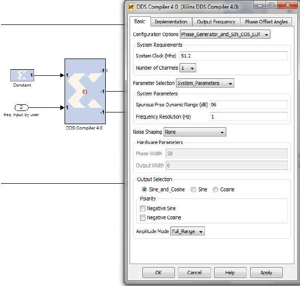
Figure 19: DDS Compiler and its Parameters
FIR Compiler
The Xilinx FIR Compiler block implements a Multiply Accumulate based or Distributed-Arithmetic FIR filter. It accepts a stream of input data and computes filtered output with a fixed delay based on the filter configuration.
Coefficient Vector: It specifies the coefficient vector as a single MATLAB row vector. The number of taps is inferred from the length of the MATLAB row vector.
Number of Coefficients sets: The number of sets of filters coefficients to be implemented. The value specified must divide without remainder into the number of coefficients.
Single Rate: The data rate of the input and the output are the same.
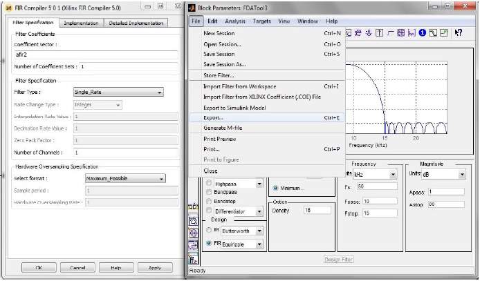
Figure 20: FIR Compiler and its Parameters
Interpolation: The data rate of the output is faster than the input by a factor specified by the Interpolation Rate Value.
Decimation: The data rate of the output is slower than the input by a factor specified in the Decimation Rate Value.
FDA Tool
This block provides the same exact filter implementation as the Digital Filter Design. The Digital Filter block implements a digital FIR or IIR filter that you design using the Filter Design and Analysis Tool (FDA Tool) GUI. This block provides the same exact filter implementation as the Digital Filter block.
The Sampling Frequency Fs that you specify in the FDA Tool GUI should be identical to the sampling frequency of the Digital Filter Design block’s input block. When the sampling frequencies of these blocks do not match, the Digital Filter Design block returns a warning message and inherits the sampling frequency of the input block.
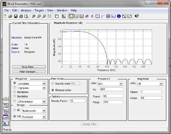
Figure 21: FDA Tool Parameters
Cordic atan
Coordinate rotation digital computer in circular vectoring mode. Complex input <x,y>new vector (m,a). It is implemented in 3 steps:
Magnitude m=kxx2+y2
Angle a=tan-1yx
Scaling factor k=1.64
Coarse angle rotation: The algorithm converges only for angles between
-π2to
π2. SO if x<0, input vector is reflected to q1 or q3 and x coordinate is non-negative.
Fine angle rotation: For rectangular to polar conversion, the resulting vector is rotated through small angle, y approximated to zero.
Number of processor element: It specifies number of iterative stages for fine rotation.
X, Y data width: It specifies the width of input x and y. The inputs x, y are signed data and same data width.
X, Y binary point position: It generated the binary point position of x and y. Both (x,y) are signed and has same binary point.
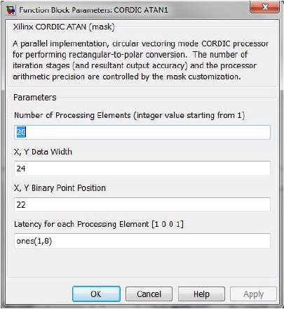
Figure 22: Cordic atan Block Parameters
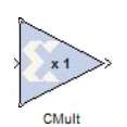
CMult
The Xilinx cmult block implements a gain operator with output equal to the product of its input by a constant value. This can be a MATLAB expression that evaluates to a constant.
Constant Value may be a constant or an expression.
Constant number of bits specifies bit location of the binary point of constant
Constant binary point position of binary point
Output type tab defines the precision of output of cmult block
Test for optimal pipelining checks if the latency period provided is at least equal to the optimum pipeline length supported for the given configuration of the block.
Gateway In
The Xilinx Gateway In blocks are the input into Xilinx portion of the Simulink design, thus serving as a connector between both. These blocks convert Simulink inter, double and fixed-point data types into System Generator fixed –point type. Each block defines a top level input port in the HDL design generated by System generator. While converting a double type to a System generator fixed-point type, the Gateway In uses the selected overflow and quantization options. For overflow, the options are to saturate to the largest positive/smallest negative value, to wrap (i.e. to discard bits to the left of the most significant representable bit), or to flag an overflow as a Simulink error during simulation.
For quantization, the options are to round to the nearest representable value (or to the value furthest from zero if there are two equidistant nearest representable values), or to truncate (i.e., to discard bits to the right of the least significant representable bit). During HDL simulation an entity that is inserted in the top level test bench checks this vector and the corresponding vectors produced by gateway out blocks against the expected results.
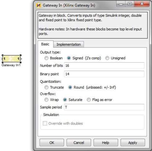
Figure 24: Gateway In and its Parameters
Multiplier
The Xilinx Multi block implements a multiplier. It computes the product of the data on its two input ports, producing the result on its output port.
Latency: This defines the number of sample periods by which the block’s output is delayed.
Saturation and Rounding of User Data Types in a Multiplier: When saturation or rounding is selected on the user data type of a multiplier, latency is also distributed so as to pipeline the saturation/rounding logic first and then additional registers are added to the core until optimum pipelining is reached and then further registers will be placed after the rounding/saturation logic. However, if latency is selected and rounding/saturation is selected, then the first register will be placed after the rounding or saturation logic and two registers will be placed to pipeline the core.
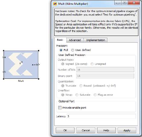
Figure 25: Multiplier Block and its Parameters
.8. Modulation and Demodulation
The process by which some characteristic of a carrier is varied in accordance with a modulating wave which causes a shift of the range of frequencies in a signal is known as modulation. A common form of the carrier is a high frequency sinusoidal wave which contains the information to be transmitted. The baseband signal is referred to as the modulating wave, and the result of the modulation process is referred to as the modulated wave. Modulation is performed at the transmitting end of the communication system. At the receiving end of the system, the original baseband signal is restored by the means of a process known as demodulation.
A device that performs modulation is known as a modulator and a device that performs the inverse operation of modulation is known as a demodulator. A device that can do both operations is a modem.
In analog modulation, the baseband signal is transferred over an analog band-pass channel at a different frequency. In digital modulation, a digital bit stream is transferred over an analog band-pass channel.
Analog Modulation Techniques
Analog Modulation Techniques, also known as Continuous Wave Modulations Systems are of two types, amplitude modulation and angle modulation. In amplitude modulation, the amplitude of the sinusoidal carrier wave is varied in accordance with the baseband signal. In angle modulation, the angle of the sinusoidal carrier wave is varied in accordance with the baseband signal.
Common analog modulation techniques are:
- Amplitude modulation (AM)
- Double-sideband modulation (DSB-AM)
- Double-sideband suppressed-carrier transmission (DSB-SC)
- Single-sideband modulation (SSB-AM)
- SSB suppressed carrier modulation (SSB-SC)
- Vestigial sideband modulation (VSB-AM)
- Angle Modulation
- Frequency Modulation (FM)
- Phase Modulation (PM)
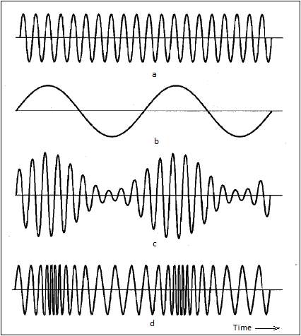
Figure 26: a) Carrier Wave b) Modulating Sinusoidal Wave c) Amplitude Modulated Wave
d) Frequency Modulated Wave[10]
Amplitude Modulation
Amplitude Modulation is the process where the amplitude of the carrier signal is varied in accordance to the instantaneous amplitude of the modulating signal. In radio communication, a continuous wave radio-frequency signal (a sinusoidal carrier wave) has its amplitude modulated by an audio waveform before transmission. In the frequency domain, amplitude modulation produces a signal with power concentrated at the carrier frequency and two adjacent sidebands. Each sideband is equal in bandwidth to that of the modulating signal, and is a mirror image of the other. Amplitude modulation resulting in two sidebands and a carrier is called “double-sideband amplitude modulation” (DSB-AM).
Double Side Band AM (DSB-AM)
Modulation
A carrier wave is modelled as a sine wave.
ct=A.sin(ωct+φc)
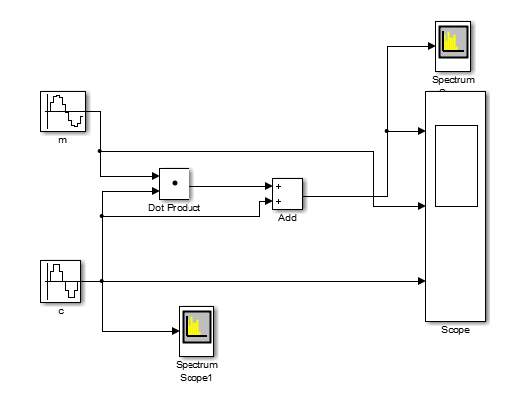
Figure 27: Amplitude Modulation and Demodulation
In which the frequency in Hz is given by
ωc2π
The constants
Aand
φcrepresent the carrier amplitude and initial phase respectively. For simplicity, their respective values can be set to 1 and 0.
Let
mtrepresent an arbitrary waveform that is the message signal to be transmitted, and let the constant M represent its largest magnitude.
mt=M.cos(ωmt+φ)
The message might be just a simple audio tone of frequency:
ωc2π
It is assumed that
ωm≪ ωcand that
minmt=-M
yt=A.1+M.cosωmt+φ.sin(ωct)
‘
A’ demonstrates the modulation index.
The values
A=1and
M=0.5produce y(t), depicted by the graph (labelled “50% Modulation”)
In this example,
ytcan be trigonometrically manipulated into the following (equivalent) form:
yt=A.sinωct+AM2[sinωc+ωmt+φ+sin(ωc+ωmt-φ)]
Therefore, the modulated signal has three components: a carrier wave and two sinusoidal waves (known as sidebands), whose frequencies are slightly above and below
ωc.
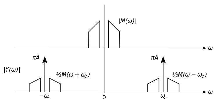
Figure 28: Double Side Band Specta of baseband and AM Signals[11]
Power and Spectrum Efficiency
In terms of positive frequencies, the transmission bandwidth of AM is twice the signal’s original (baseband) bandwidth; both the positive and negative sidebands are shifted up to the carrier frequency. Thus, double-sideband AM (DSB-AM) is spectrally inefficient since fewer radio stations can be accommodated in a given broadcast band.
If
fcis the carrier frequency and
fmis the maximum modulation frequency then the power spectrum appears as shown in Figure.
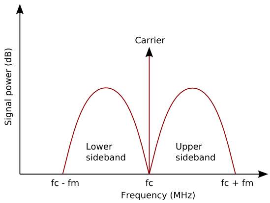
Figure 29: Power of an AM plotted against frequency[12]
Modulation Index
The AM modulation Index is the measure of the amplitude variation surrounding an unmodulated carrier. As with other modulation indices, in AM this quantity (also called “modulation depth”) indicates how much the modulation varies around its “original” level. For AM, it relates to variations in carrier amplitude and is defined as:
h=peak value of m(t)A=MA
Where
Mand
Aare the message amplitude and carrier amplitude, respectively.
For
h=0.5, carrier amplitude varies by 50% above (and below) its unmodulated level; for
h=1.0, it varies by 100%. To avoid distortion, modulation depth must not exceed 100 percent. Transmitter systems will usually incorporate a limiter circuit to ensure this.
Variations of a modulated signal with percentages of modulation are shown below. In each image, the maximum amplitude is higher than in the previous image.
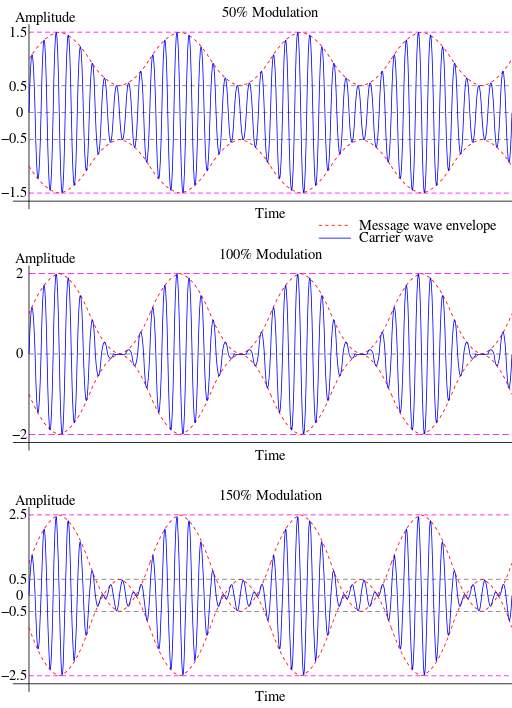
Figure 30: Modulated Depth: Unmodulated carrier has amplitude of 1[13]
Demodulation
Product Detector: A product detector is a type of demodulator used for AM and SSB Signals. Rather than converting the envelope of the signal into the decoded waveform like an envelope detector, the product detector takes the product of the modulated signal and a local oscillator, hence the name. A product detector is a frequency mixer.
Product detectors can be designed to accept either IF or RF frequency inputs. A product detector which accepts an IF signal would be used as a demodulator block in a super heterodyne receiver, and a detector designed for RF can be combined with an RF amplifier and a low-pass filter into a direct-conversion receiver.
The simplest form of product detector mixes (or heterodynes) the RF or IF signal with a locally derived carrier (the Beat Frequency Oscillator, or BFO) to produce an audio frequency copy of the original audio signal and a mixer product at twice the original RF or IF frequency. This high-frequency component can then be filtered out, leaving the original audio frequency signal.
Mathematical model of a simple product detector:
If
m(t)is the original message signal, then the AM signal can be shown as:
xt=C+mtcos(ωt)
Multiplying the AM signal
xtby an oscillator at the same frequency as and in phase with the carrier yields:
yt=(C+mtcosωtcosωt
This can be written as:
yt=C+mt(12+12cos2ωt)
After filtering out the high frequency component based around
cos2ωtand the DC component C, the original message signal will be recovered.
Advantages
- AM transmitters are less complex
- AM receivers are simple, detection is easy
- AM receivers are cost efficient
- AM waves travel a long distance
Drawbacks
- Performance of AM is very poor in presence of noise
- High signal-to-noise ratio
- Bandwidth inefficient system
- Power inefficient system
Applications
- Radio Broadcasting
- Picture transmission in TV system
- Telephone subscriber call
Double Side Band – Suppressed Carrier
In AM modulation, transmission of carrier consumes lot of power. Since, only the side bands contain the information about the message, the carrier can be suppressed. This results in a DSB-SC wave.
In DSB-SC
- Frequencies produced by amplitude modulation are symmetrically spaced above and below the carrier frequency
- The carrier level is reduced to the lowest practical level, ideally completely suppressed.
In the double-sideband suppressed-carrier transmission (DSB-SC) modulation, unlike AM, the wave carrier is not transmitted; thus, a great percentage of power that is dedicated to it is distributed between the sidebands, which imply an increase of the cover in DSB-SC, compared to AM, for the same power used.
Modulation
DSB-SC is generated by a mixer. This consists of an audio source combined with the frequency carrier.
Vmcosωmt×Vccosωct=VmVc2cosωc+ωmt+cos(ωc-ωmt)
On the left hand side of the equation, the first term is audio and the second term is the carrier. While, on the right hand side of the equation the first term is the USB and the second term is the LSB.
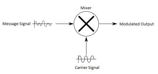
Figure 31: DSB-SC Generation[14]
Demodulation
The audio frequency and the carrier frequency must be exact for demodulation otherwise distortion is obtained. DSB-SC can be demodulated if modulation index is less than unity.
Mathematical representation of DSB-SC
Let
mtbe the original message signal,
vtcan then be written as:
vt=st.cosωct+φ
vt=mt*Accosωctcos(ωct+φ)
vt=mt2*Accos2ωct+φcos(φ)
If, the demodulator has constant phase, the original signal is reconstructed by passing
vtthrough an LPF.
A coherent demodulator is used. The local oscillator present in the demodulator generates a carrier which has the same frequency and phase as that of the carrier in the modulating signal.
Insert image of Simulink DSB-SC mod and Demod
Spectrum
This is basically an amplitude modulation wave without the carrier therefore reduces power wastage, giving it a 100% efficiency rate. This is an increase compared to normal AM transmission (DSB), which has a maximum efficiency of 33.33%. Efficiency is defined as:
E=Sideband PowerSideband Power+Carrier Power
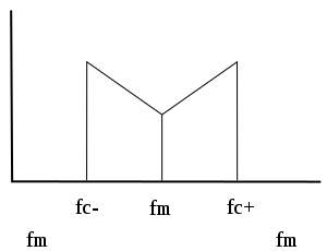
Figure 32: Spectrum Plot of a DSB-SC Signal
Advantages
- Due to carrier suppression, a lot of power is saved (66.66% of power is saved)
Disadvantages
- Information contained by two side bands is same which is redundant
Single Side Band Modulation
Single-sideband (SSB) or Single-sideband suppressed-carrier (SSB-SC) modulation is a refinement of amplitude modulation that more efficiently uses electrical power and bandwidth.
Amplitude modulation produces a modulated output signal that has twice the bandwidth of the original baseband signal. Single-sideband modulation avoids this bandwidth doubling, and the power wasted on a carrier, at the cost of somewhat increased device complexity and more difficult tuning at the receiver.
Figure 33: SSB Modulation and Demodulation
Advantages
- Less bandwidth requirements
- Lots of power saving. This is due to the transmission of only one side band component
- Reduced interference of noise. This is due to reduced bandwidth
- At 100% modulation, the percent power saving is 83.33%
Disadvantages
- Generation and reception of SSB signal is complicated
- SSB transmitter and receiver should have excellent frequency stability
Applications
- Speech transmission.
- Land and air mobile communications, telemetry
- Military communication, navigation and amateur radio
- Point to point communication applications
Frequency Modulation
Frequency modulation (FM) conveys information over a carrier wave by varying its instantaneous frequency. This contrasts with amplitude modulation, in which the amplitude of the carrier is varied while its frequency remains constant. In analog applications, the difference between the instantaneous and the base frequency of the carrier is directly proportional to the instantaneous value of the input-signal amplitude.
Frequency modulation is known as phase modulation when the carrier phase modulation is the time integral of the FM signal. It is used in telemetry, radar, seismic prospecting and newborn EEG seizure monitoring. Also, FM is widely used for broadcasting music and speech, two-way radio systems, magnetic tape-recording systems and some video-transmission systems. In radio systems, frequency modulation with sufficient bandwidth provides an advantage in cancelling naturally-occurring noise as noise does not affect the frequency of the signal as that t affects the amplitude. Frequency modulation (FM) is a type of angle-modulated signal. A conventional angle-modulated signal is defined by the following equation:
XAngle(t)≜Accos(ωct+Pt)
Where the carrier frequency (rad/s) is
ωc,
Acis constant amplitude factor,
Ptis the modulating input signal and
mtis the original message signal.
For FM, the relation of
m(t)to
P(t)is given by:
P(t)FM=Df∙∫-∞tm(ξ)dξ
Where
Dfis a constant measured in radians/volt-seconds.
Taking the time derivative of both sides of Equation it is readily seen that the
Message signal
mtis the derivative of the modulating signal
P(t)FM.
By applying Leibniz’s rule
∂∂tP(t)FM=Df∙∂∂t∫-∞tmξdξ
∂∂tP(t)FM=Df∙m(t)
By observing the above equation it can be seen that the instantaneous phase of an FM signal is directly related to the message signal
m(t). The FM equation now takes the following form:
XFMt≜Accosωct+PtFM=Accos(ωct+Df∫-∞tm(ξ)dξ
The instantaneous frequency of the FM signal in equation is
ΔF=12π∂P(t)FM∂t
Now that
ΔFis a non-negative number measured in Hertz. The maximum frequency deviation of an FM signal, denoted Δ F max, is directly proportional to the amplitude of the input signal. The equation for maximum frequency deviation is given below:
ΔFmax=12πDf∙maxm(t)
Equation makes it obvious that an increase in the message
m(t)amplitude creates an increase in the maximum frequency deviation. The increase in frequency deviation also increases the bandwidth of the FM signal. The important relationship established above is that the instantaneous frequency of an FM signal can be used to directly recover the original message
m(t).
Finally, the real FM equation can also be represented as a complex FM signal through the Euler identity.
XFMt= Accos(ωct+P(t)FM
This can be written as:
XFMt=ReAc∙ejP(t)FMejωct=ReAc∙ejωct+P(t)FM
In Phase and Quadrature Phase
When a real signal for example
Asinωtis transmitted over the air it is subject to noise and distortion in its phase. For synchronous detection, we use complex signals which contain two orthogonal components,
I=Acos(φ)and
Q=Asin(φ). From this, the signal magnitude
Aand phase angle
φcan be calculated as:
A2=I2+Q2
φ=tan-1(QI)
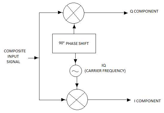
Figure 34: Obtaining I and Q Components[15]
Amplitude Modulation using IQ
The amplitude of a complex signal is obtained by squaring the I and Q phase components of the signal.
Received Am signal is:
At=V+m(t)cosωt+φ
Where,
Vis the amplitude of the carrier signal,
ωis its frequency and
mtis the message signal.
Demodulation
The In phase component is,
I=At*cosωt
I=12*V+m(t)*cos2ωt+φ+cosφ
This is passed through a low pass filter with cut-off
2ω. Therefore,
I=12*V+m(t)*cosφ
Quadrature phase component is:
Q=At*sinωt
Q=12*V+m(t)*[sin2ωt+φ+sinφ]
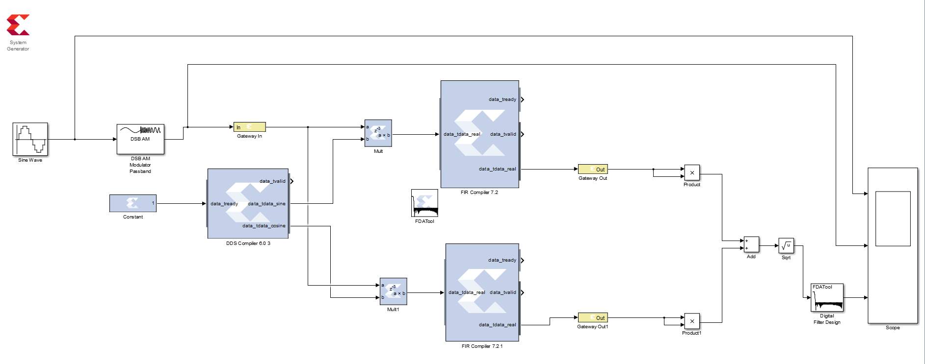
Figure 35: Amplitude Modulation using IQ Components
This is passed through a low pass filter with cut-off
2ω. Therefore,
Q=12*V-m(t)*sinφ
Squaring these components and adding them, we get:
I2+Q22= 14*V2*sin2φ+cos2φ+14*m2t*sin2φ+cos2φ2
I2+Q22=14*V2+14*m2t2
Frequency Modulation using IQ
An FM signal at baseband, or zero frequency, is the result of “mixing out” the carrier frequency from the FM signal, as shown in Figure. Thus, the carrier frequency no longer appears in the FM equation. For this reason, the representation of a complex-valued FM signal at baseband is derived. The generation of complex data is the result of mixing the FM signal with a cosine and sine local oscillator (LO). This process can be derived mathematically by using the complex version of the FM equation. The mixing process is a simple multiplication of signals. For baseband results, both mixers oscillate at the FM carrier frequency c. The total mixing operation produces a real (in-phase) and imaginary (quadrature-phase) baseband component. Adding the in-phase and quadrature-phase components will result in the complex baseband FM signal.
Received FM signal is:
Ft=V*cosωt+∫mt.dt
Where,
Vis the amplitude of the carrier signal,
ωis its frequency and
mtis the message signal.
Demodulation
The In phase component is:
I=Ft*cos(ωt)
I=V2*cos∫mt.dt+cos2ωt+∫mt.dt
This is passed through a low pass filter with cut-off
2ω. Therefore,
I=V2*cos∫mt.dt
Quadrature phase component is,
Q=Ft*sin(ωt)
Q=V2*sin∫mt.dt-sin2ωt+∫mt.dt
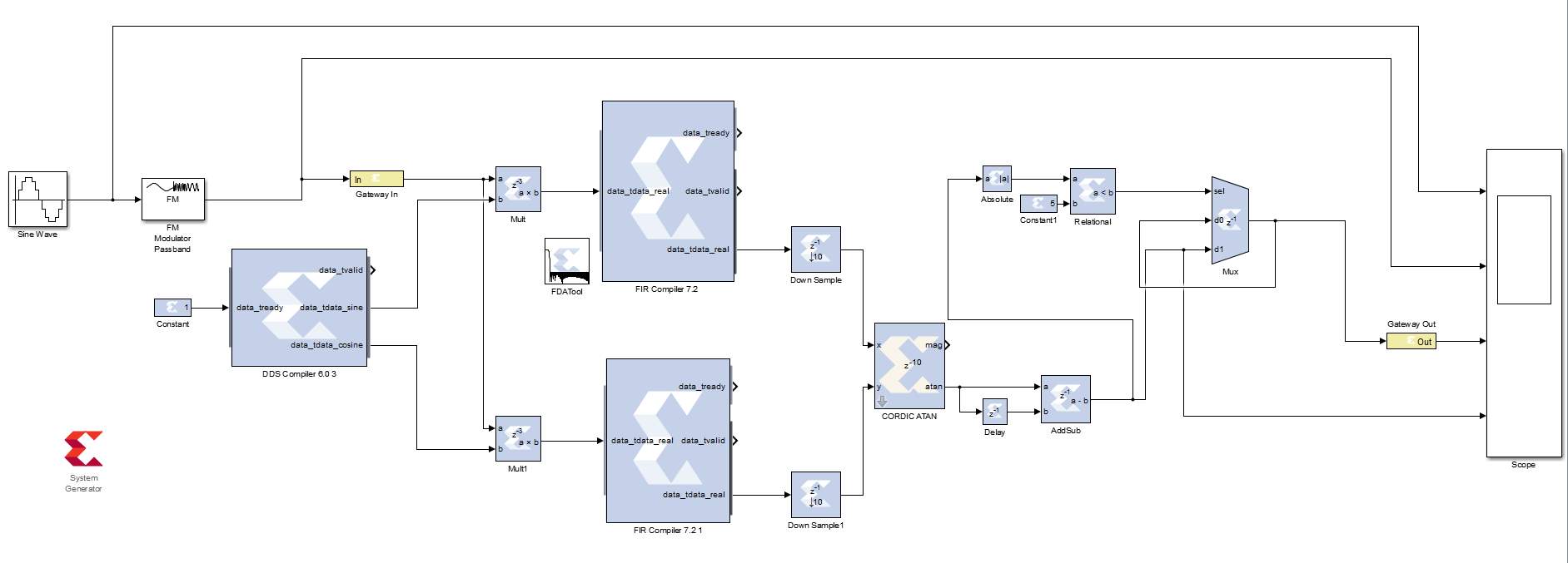
Figure 36: Frequency Modulation using IQ Components
This is passed through a low pass filter with cut-off
2ω. Therefore,
Q=V2*sin∫mt.dt
Now, obtain Q/I component and pass it through arctan block.
tan-1Q/I=tan-1tan∫mt.dt=∫mt.dt
This is then passed through a differentiator to obtain message
mt.
This method in comparison with the earlier method is efficient because it does not depend on the input frequency and amplitude
Mixed Demodulator
Frequency modulation using normal method or phase method requires a differentiator at the end to obtain the message signal where, an error that occurs even at one sample propagates throughout the signal. To avoid this we use mixed demodulator.
Mathematically this is obtained as follows.
After the I and Q components of received signal are obtained we get,
In=Vcosφn; Qn=Vsin φn; In-1=Vcosφn-1; Qn-1=Vsin φn-1
Where,
Vis the carrier amplitude and
φn=∫mt.dtLet,
P=In*In-1
P1=Qn*Qn-1
P2=Qn*In-1
P3=In*Qn-1
P2-P3=V2sin(φn-φn-1)
P+P1=V2cos(φn-φn-1)
Dividing the two equations, we get:
(P2-P3)/(P+P1)=tan(φn-φn-1)
Obtaining arc tan for the equation we get the differential output directly as,
(φn-φn-1)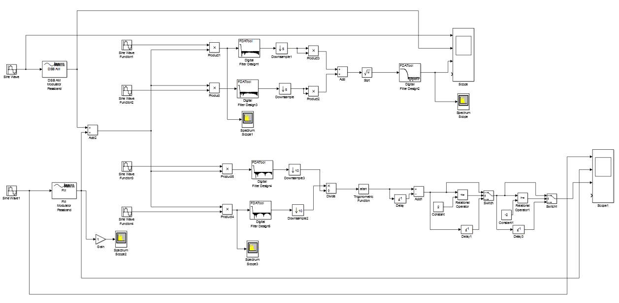
Figure 37: Mixed Demodulator for FM
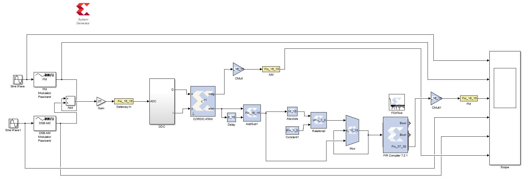
Figure 38: AM and FM combined into a single hardware Model
Digital Modulation Techniques
In digital modulation, an analog carrier signal is modulated by a discrete signal. Digital modulation methods can be considered as digital-to-analog conversion or modulating an analog signal using digital bits, and the corresponding demodulation as analog-to-digital conversion.
A simple example: A telephone line is designed for transferring audible sounds, for example tones, and not digital bits. Computers may however communicate over a telephone line by means of modems, which are representing the digital bits by tones, called symbols. If there are four alternative symbols, the first, second third and fourth symbols may represent the bit sequence 00, 01, 10 and 11 respectively. If the modem plays a melody consisting of 1000 tones per second, the symbol rate is 1000 symbols/second, or baud. Since each tone (i.e., symbol) represents a message consisting of two digital bits in this example, the bit rate is twice the symbol rate, i.e. 2000 bits per second.
Fundamental Digital Modulation Methods
The most fundamental digital modulation techniques are based on keying:
- In the case of PSK (phase-shift keying), a finite number of phases are used
- In the case of FSK (frequency-shift keying), a finite number of frequencies are used
- In the case of ASK (amplitude-shift keying), a finite number of amplitudes are used
- In the case of QAM (quadrature amplitude modulation), a finite number of at least two phases, and at least two amplitudes are used
9. Methodology
To implement the Monitoring Receiver System on an FPGA, a general methodology has been presented which can be used for other systems as well. We have used Simulation as our main feature of the process. Simulation is the process of carrying out alternate model based architectures towards terminal specifications and then to test them using comprehensive list of test vectors. At the end of this process an architecture can be finalised which optimises performance, reliability and cost. The finalised architecture must also be supported by the industry for a decade so that the solution can be updated and upgraded.
The methodology can be divided into 3 sections. Section I covers the design and verification of the system model using MATLAB Simulink software tool. Section II covers the design and verification of the system model using Xilinx System Generator Block Sets available in MATLAB Simulink in order to make it compatible with hardware evaluation board. The representation of the two architectures used in Section I and II is different although the output shall remain the same. After this, this final testing and verification is done using FPGA which has been discussed in Section III. The final results of the system model are presented in the next chapter.
SECTION I
Design using MATLAB Simulink
The first step was to create the model of the monitoring system on MATLAB Simulink using the available blocks. The main focus was on the receiver part of the whole communication system hence, in-built blocks were used for the transmission portion of the system such as modulators. The receiver logic was made in a systematic fashion. The received signal is fed into an ADC i.e. Analog to Digital convertor, followed by a DDC (Digital-Down Convertor). The signal is converted into its In phase and quadrature phase for the process of demodulation.
SECTION II
Design using Xilinx System Generator Blocks in MATLAB
Block Description
Antenna
An antenna is a specialized transducer that converts radio-frequency (RF) fields into alternating current (AC) or vice-versa.[16] In other words, it converts EM waves into electrical signals. This project requires a receiving antenna which intercepts RF energy and delivers AC to electronic equipment. The antenna used in this model is an Omni-directional antenna. It is tuned to a RF frequency in the range 30 to 3000MHz.
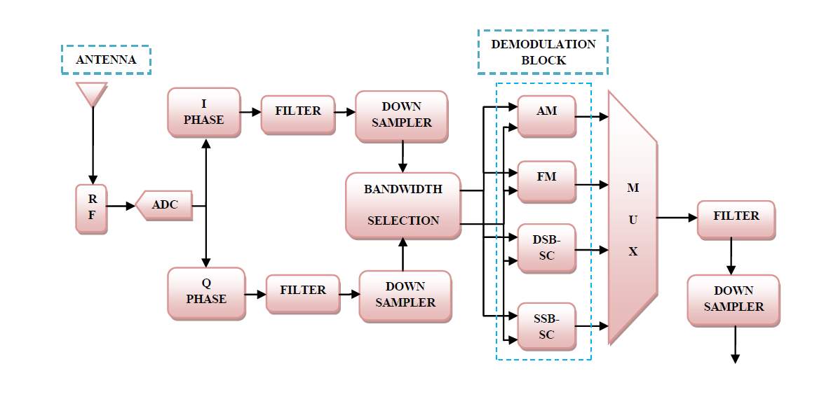
Figure 39: Block Diagram of System Model
RF Module
The RF Module is also called RF tuner. A tuner is a subsystem that receives radio frequency (RF) transmissions like radio broadcasts and converts the selected carrier frequency and its associated bandwidth into a fixed frequency that is suitable for further processing[17]. Therefore, the RF tuner converts the received signal into a fixed frequency also known as Intermediate frequency (IF). It is required as the received signals from antenna may be at a very high frequency range i.e. somewhere in MHz or GHz.
The received signal is fed to the RF block which is the first block of the receiver station. The RF block consists of a mixer and a band pass filter. The mixer converts the high frequency signal to the IF frequency range. Then the signal passes through the band pass filter (BPF) which is tuned to the desired frequency range. The filtered signal is sent to the ADC which samples it at IF frequency range.
For examplelet’s say thatthe received signal had a frequency of 100MHz. It is difficult to perform demodulation at such high frequencies. Also ADCs are incapable of acquiring high frequency signals. Hence, the 100 MHz signal is limited to 10.7 MHz which makes the further demodulation stages flexible where the components in that stage’s are of capable to allow the frequency limited signal. The IF frequency of 10.7 MHz (IF range for FM) is a pre-defined value that is taken into consideration.
ADC
In order to provide bit-accurate simulation of hardware, System Generator blocks operate on Boolean, floating-point, and arbitrary precision fixed-point values. The connection between Xilinx blocks and non-Xilinx blocks is provided by gateway blocks. The Gateway In converts a double precision signal into a Xilinx signal, and the Gateway Out converts a Xilinx signal into double precision. Simulink continuous time signals must be sampled by the Gateway
In MATLAB Simulink, we have used Gateway In as a 14 bit ADC. Out of 14 bits 13 bits are used as the binary digits and rest 1 bit is used as either signed or unsigned bit.
Analog-to-digital conversion is an electronic process in which a continuously variable (analog) signal is changed, without altering its essential content, into a multi-level (digital) signal. The output of the ADC has defined levels or states. The number of states is almost always a power of two — that is, 2, 4, 8, 16, etc. The simplest digital signals have only two states, and are called binary.
Digital signals propagate more efficiently than analog signals, largely because digital impulses, which are well-defined and orderly, are easier for electronic circuits to distinguish from noise, which is chaotic. This is the chief advantage of digital modes in communications.
An ADC may also provide an isolated measurement. The reverse operation is performed by a Digital-to-Analog Converter (DAC). Analog-to-Digital converters are used virtually everywhere where an analog signal has to be processed, stored, or transported in digital form. Very fast ADCs are incorporated at new areas like software defined radio (SDR).
ADC’s can be illustrated by different parameters. They are:
- Resolution: The resolution of the converter indicates the number of discrete values it can produce over the range of analog values. The values are usually stored electronically in binary form, so the resolution is usually expressed in bits. Normally, the number of voltage intervals is given by,
N=2M; where M is the ADCs resolution in bits. - Accuracy: An ADC has several sources of errors. Quantization error and (assuming the ADC is intended to be linear) non-linearity are intrinsic to any analog-to-digital conversion. Rather from the mentioned errors there is also one type of error called
- Aperture error which is due to a clock jitter and is revealed when digitizing a time-variant signal (not a constant value).
- Quantization error: Quantization error (or quantization noise) is the difference between the original signal and the digitized signal. Hence, the magnitude of the quantization error at the sampling instant is between zero and half of one LSB. Quantization error is due to the finite resolution of the digital representation of the signal, and is an unavoidable imperfection in all types of ADCs.
- Sampling Rate: The analog signal is continuous in time and it is necessary to convert this to a flow of digital values. It is therefore required to define the rate at which new digital values are sampled from the analog signal. The rate of new values is called the sampling rate or sampling frequency of the converter. The sampling frequency is such that it satisfies Nyquist theorem.
There are different types of ADC’s present in the DSP field. These ADC’s are classified according to their specifications and user defined outputs. Some kinds of ADC’s are:
- Direct-Conversion ADC.
- Successive-Approximation ADC.
- Pipeline ADC.
- Sigma-Delta ADC, etc.
- Flash ADC
Our project uses the pipeline ADC.
I-Phase and Q-Phase
Quadrature Signals are used in modulating processes for their various advantages. A quadrature signal is a two-dimensional signal whose value at some instant in time can be specified by a single complex number having two parts; what we call the real part and the imaginary part. In other terms, the in phase and quadrature phase are same as real and imaginary part.
An IQ modulator can actually create AM, FM and PM. When you modulate a carrier with a message signal waveform that changes the carrier’s frequency slightly, you can treat the modulating signal as a phasor. It has both a real and an imaginary part, or an in-phase (I) and a quadrature (Q) part. Now construct a receiver that locks to the carrier, and you can decipher information by reading the I and Q parts of the modulating signal. One of the major advantages of I and Q phase modulation is that it takes care of the phase and hence synchronization at the receiver end is not a problem. A few more advantages are stated below:
- Synchronization is possible at receiver.
- Removes noise.
- Power efficient.
- Wide band analog signals can be captured for a fixed sampling frequency value.
- Quadrature sequences make FFT processing more efficient due to wide frequency range coverage.
- Since quadrature sequences are effectively oversampled by a factor of two, signal squaring operations are possible without the need of up-sampling
- Phase of the signal is known, enabling coherent processing
- Quadrature sampling also helps measure instantaneous magnitude and phase of a signal during demodulation.
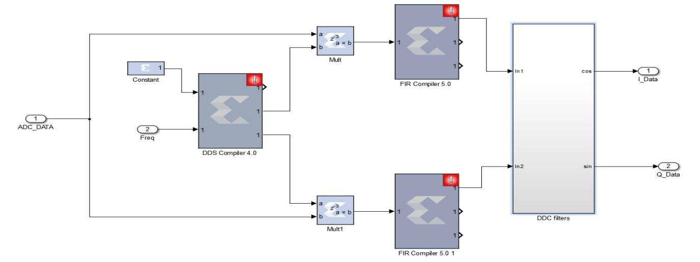 Figure 40: DDC: I and Q Components obtained from multiplying received signal with signal from DDS
Filter
Electronic filters are analog circuits which perform signal processing functions, specifically to remove unwanted frequency components from the signal, to enhance wanted ones, or both. Filters can be active or passive, analog or digital, high-pass or low-pass or band-pass or band-stop or all-pass, infinite impulse response or finite impulse response and linear or non-linear. In this model we use band pass filters which pass frequencies within a certain range and rejects (attenuates) frequencies outside that range. Filtering results in averaging the samples. A series of filter blocks and CMult blocks are used to filter out each sample and normalize the output.
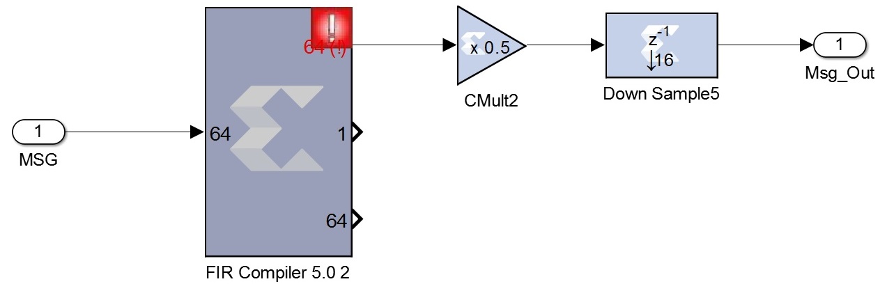
Down Sampler
The Nyquist Theorem, also known as the Sampling Theorem forms the fundamental basis of sampling. Nyquist Theorem states that the sampling frequency must be greater than or equal to twice the highest frequency component of the message signal.
Fs≥2fm
If Fs is greater than 2Fm then the signal is oversampled. Oversampling relaxes filter requirements. On the other hand, it requires higher speed ADCs and increases data rate in digital processing. Therefore sampling rate is varied at different stages using up/down samplers.
In the case of quadrature sampling, the input signal is split into in-phase and quadrature-phase components. Their bandwidth is half of the bandwidth of the original signal. Thus, quadrature sampling reduces the required sampling rate. The demodulation of phase or frequency modulated signals needs both in-phase and quadrature samples because these components have different information.
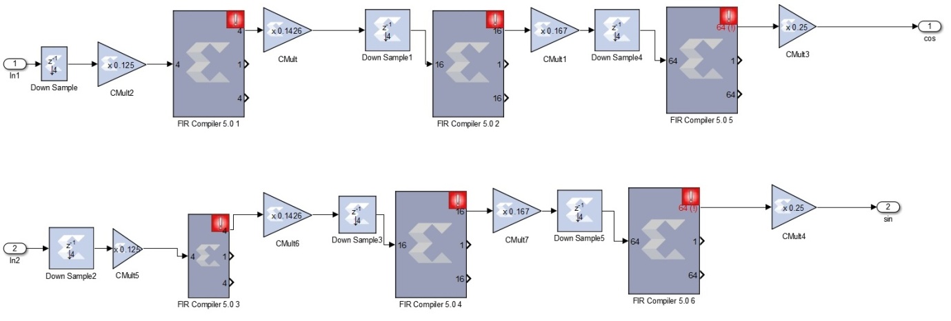
Figure 42: DDC Filters for multi-stage Down-Sampling
RF bands of radio systems have band-pass characteristics instead of low-pass characteristics. Band-pass sampling, or sub-sampling, also utilizes the Nyquist theorem. It is necessary that information in any Nyquist zone will not interfere with information in other Nyquist zones. By using this approach, down conversion is provided along with anti-aliasing filters by the sampling process.
Bandwidth Selection
The bandwidth of the system is varied using the bandwidth selection module. Selection is done on the basis of type of modulation used and the message signal frequencies. The detection of type of modulation scheme can be done in two ways, manually by visual observation or by a PC using analyzing software. Either ways the output remains the same. After detection, the signal is sent to the MUX from where the appropriate bandwidth is selected for further processing.
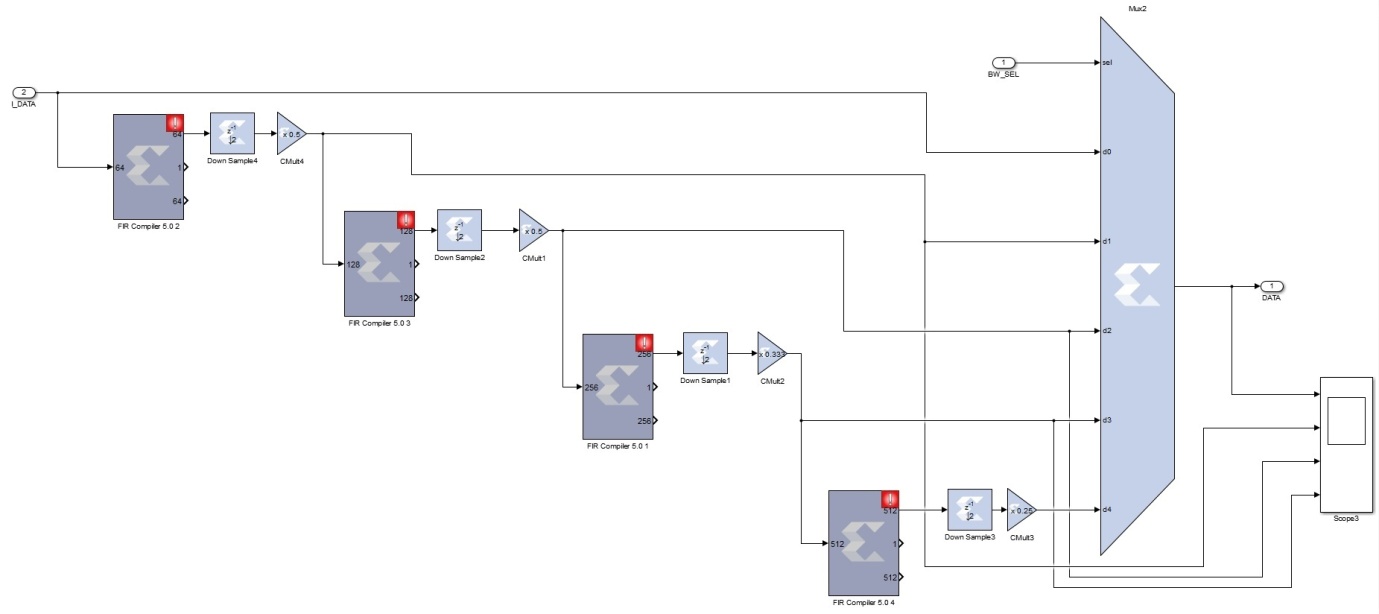
Figure 43: Bandwidth Selection Block
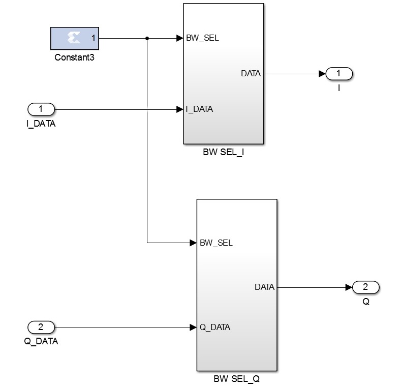
Figure 44: Bandwidth Selection for both I and Q components
| Selection Line
S2 S1 S0 |
Sampling Frequency
Fs (in KHz) |
Bandwidth
(in KHz) |
| 000 | 800 | 100 |
| 001 | 400 | 50 |
| 010 | 200 | 25 |
| 011 | 100 | 12.5 |
| 100 | 50 | 6.25 |
Table 3: Output of Bandwidth Selection Block
This block has the implementation of different demodulation techniques. The analog demodulation techniques available are DSB-AM, DSB-SC AM, SSB-SC LSB AM, SSB-SC USB AM and FM. They are constructed using techniques described in chapter 8 – Modulation and Demodulation. Demodulation of FM and AM can be obtained from a single Cordic tan block and DSB and SSB can be obtained from AM directly.
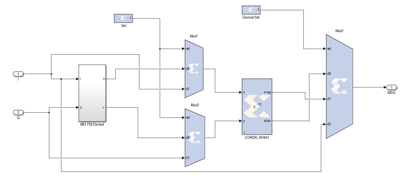
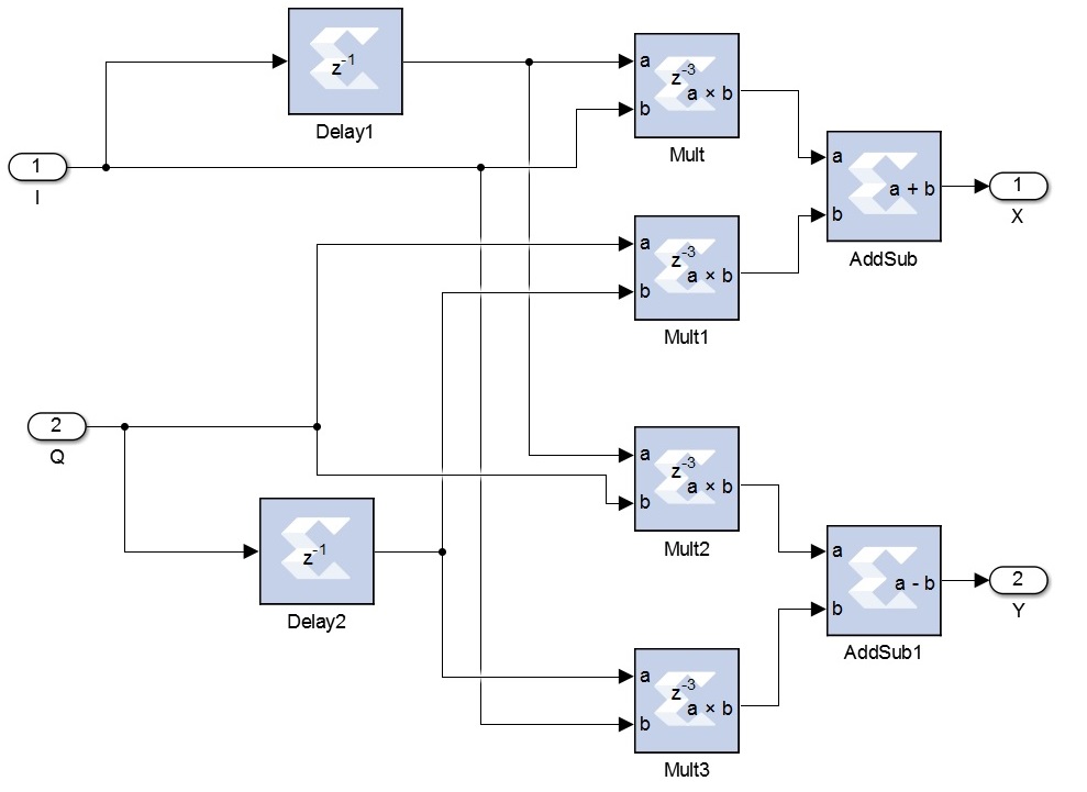
Multiplexer
All the demodulated outputs are multiplexed at the end to produce a single output at a time on the receiver end. The output is selected based on the selection line.
| Selection Line
S1 S0 |
Demodulated Output Type |
| 00 | DSB AM |
| 01 | DSB-SC AM |
| 10 | SSB AM |
| 11 | FM |
Table 4: Selection Line and MUX Output
Working
The RF block receives a number of baseband signals that are modulated using different modulation techniques. The signal of our interest lies between 30 – 1000MHz. For simulation purpose, since we do not have a RF tuner, we have generated a signal using DSP hardware; which has a sampling rate of 51.2 MHz and an Intermediate frequency of 10.7MHz. The value of sampling frequency is so chosen such that the message signal retrieved at the output after down-sampling is at 50 KHz.
We have used in-built modulation blocks from MATLAB as this project mainly focuses on the receiver end of the communication system. This signal is analog in nature and hence is required to be converted to digital bits for further processing. The software platform used in the project is Xilinx’s System Generator. Hence we use Gateway In which performs the ADC operation and at the same time acts as a compiler between Matlab blocks and System Generator blocks.
The output of gateway is fed to the IQ block whose output gives us the in-phase and quadrature-phase components. In this block the Direct Digital Synthesizer (DDS) generates signals required for obtaining I and Q components. The DDS is made programmable where the user can enter the frequency to be generated at the time of the execution of the model.
The signal is then sent to the series of filters and down samplers where the sampling frequency is reduced from 51.2 MHz to 800 KHz with a bandwidth of 100 KHz. The signal out of this block is fed to the bandwidth selector where different bandwidths and sampling frequencies are provided to be selected as per user’s choice.
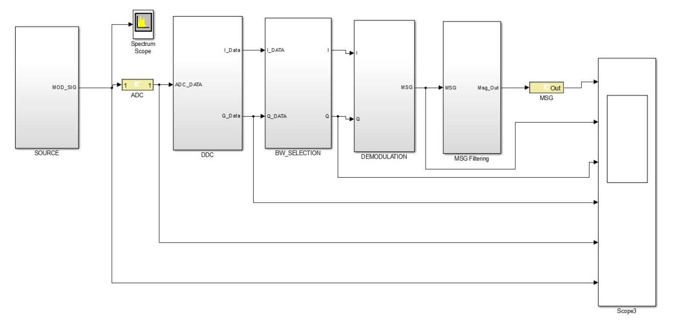
Figure 47: Model of Monitoring Receiver
The output from the bandwidth selection bock is fed to the Demodulation block where the actual processing takes place for demodulation techniques. This block has demodulation implemented for various analog modulation techniques. Output of this block directly gives the demodulated output.
The outputs of all the demodulation schemes are given to a Multiplexer, which gives the appropriate output decided on the basis of a selection line. This output is the recovered message signal that was transmitted from which information can be extracted.
Using a multiplexer and a programmable DDS block enables the user to select the type of demodulation technique so as to retrieve the message signal. The down samplers at the output end ensure that the message signal obtained has a sampling frequency of 50 KHz for any technique implemented.
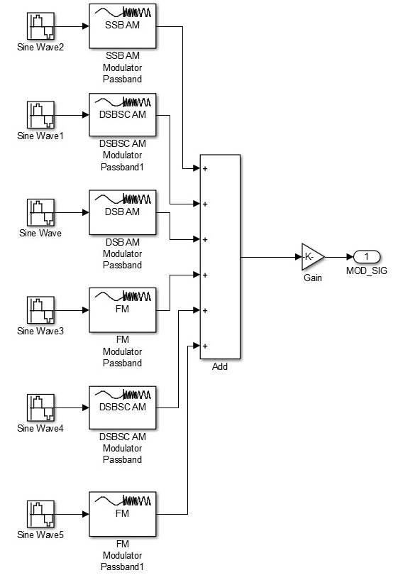
Figure 48: Signal Sources for the Monitoring Receiver
| System Specifications | |
| Frequency Range | 30 – 1000 MHz |
| Intermediate Frequency | 10.7 ± 5 MHz |
| Signal Bandwidth | 10MHz |
| Sampling Frequency | 51.2 MHz |
| Bandwidth Selection Range | 100KHz to 6.25KHz |
| Demodulation Techniques | AM, DSB – SC, SSB, FM |
| Message Signal Frequency | 50KHz |
| ADC | 14 bit |
| Values used for Testing | |
| Carrier Frequency | 10.7KHz |
| Message Frequency for AM | 1KHz |
| Modulation Index | 0.8 |
| Message Frequency for FM | 1KHz |
| Frequency Deviation | 5KHz |
Table 5: System Specifications
10. Design Verification Using FPGA
Field Programmable Gate Array (FPGA) chips with ever increasing sizes and speeds allow designers to develop large, high-speed digital systems for a specific application very quickly. These design flows must utilize the capabilities of Hardware Description Languages, synthesis and co-simulation to achieve these goals.
Hardware Description Language (HDL) such as Verilog and VHDL have been developed that allows the behavioral and structural description of a digital system in a form that can be read and simulatedSome tools have been developed that operate on more complex HDL description and perform RTL data path design, scheduling and assignment operations, but these tools generally perform best on dataflow applications like Digital Signal Processing computations.
FPGA Design Flow
The design flow for ASICs differs depending on the quality of the existing code. You must analyse the ASIC design to determine if the code meets speed and area requirements for FPGAs. Additionally, you should structure the design hierarchy for FPGA implementation.
Figure 49: FPGA Design Flow[18]
Design Entry
There are different techniques for design entry. Schematic based, Hardware Description Language and combination of both etc. Schematic is chosen when the system deals more with hardware otherwise when the design is complex or is described in an algorithm way, HDL is chosen. Language based entry is faster but lag in performance and density.
HDLs represent a level of abstraction that can isolate the designers from the details of the hardware implementation. Schematic based entry gives designers much more visibility into the hardware. It is the better choice for those who are hardware oriented. Another method but rarely used is state-machines. It is used when the design is a series of states. But the tools for state machine entry are limited.
HDL based design entry has been selected as an ideal option for this project. Based on this Register transfer Level (RTL) simulation of the design was performed.
Synthesis
Synthesis is the process of mapping the VHDL behavioural models into logic gate implementations. Synthesis tools have special optimization algorithms for Xilinx FPGAs. It accepts VHDL or Verilog code and generates a device Netlist for each design element. It consists of library parts in the chosen technology in the format EDIF (Electronic Design Interchange Format) VHDL, Verilog or XNF.
Synthesis process checks for syntax errors and analyzes the hierarchy of the design which ensures that the design is optimized for the design architecture. The resulting netlist(s) is saved to an NGC (Native Generic Circuit) file (for Xilinx® Synthesis Technology (XST)).
Implementation
This process consists of a sequence of three steps:
- Translate
- Map
- Place and Route
translate process combines all the input netlists and constraints to a logic design file. This information is saved as a NGD (Native Generic Database) file. This can be done using NGD Build program. Defining constraints means assigning the ports in the design to the physical elements (ex. pins, switches, buttons etc) of the targeted device and specifying time requirements of the design. This information is stored in a file named UCF (User Constraints File). Tools used to create or modify the UCF are PACE, Constraint Editor Etc.
Map process divides the whole circuit with logical elements into sub blocks such that they can be fit into the FPGA logic blocks. That means map process fits the logic defined by the NGD file into the targeted FPGA elements (Combinational Logic Blocks (CLB), Input Output Blocks (IOB)) and generates an NCD (Native Circuit Description) file which physically represents the design mapped to the components of FPGA. MAP program is used for this purpose.
Place and route
After the synthesis process is complete and the fully implemented design has been functionally simulated, the next step is to place and route the design onto an FPGA. The place and route process places the sub blocks from the map process into logic blocks according to the constraints and connects the logic blocks. Ex. if a sub block is placed in a logic block which is very near to IO pin, then it may save the time but it may affect some other constraint. So a trade-off between all the constraints is taken account by the place and route process. The PAR tool takes the mapped NCD file as input and produces a completely routed NCD file as output. Output NCD file consists of the routing information. After this, it performs timing simulation.
Device Programming
Now the design must be loaded on the FPGA. The design is now converted into a format accepted by the FPGA. The routed NCD file is given to the BITGEN program to generate a bit stream (a .BIT file) which can be used to configure the target FPGA device. This can be done using a cable. Selection of cable depends on the design.
System Integration
System Integration is the final process before actual construction of the physical design. This step consists of constructing a complete schematic of the entire system which includes all FPGAs and other devices such as EPROMs, PLDs, RAMs, etc., and then performing a simulation of the system with all timing information. This is the highest level of virtual prototyping in that the model will be very close to the actual system.
Fabrication
Once the entire system is simulated and the correct functionality is achieved, the actual construction of the physical prototype can begin. This generates fuse map for the individual FPGAs. It can be downloaded to program the FPGA devices which are then placed in the prototype board that is already wire wrapped and tested, and system testing and debugging can be performed.
Generating VHDL file for MATLAB Model
To generate the VHDL code for the designed model one should modify the parameters in the System Generator hyperlink. Select HDL Netlist/NGC Netlist for configuring I/O’sin the parameter block. Then select Bitstreamfor directly dumping into the FPGA board without any configuration to be done.
Configuration for Virtex-7 FPGA
Virtex®-4 FPGAs use CMOS Configuration Latches (CCLs) to enable configurable interconnects between routing lines and logic cells. Virtex-4 FPGAs are volatile devices – they do not retain their configuration when power is removed. To configure a Virtex-4 FPGA, you must reinitialize the CCLs inside the device each time power is cycled. Power up configuration for Virtex-4 FPGAs varies by application.
In the field, customers must implement a non-volatile configuration memory solution to configure Virtex-4 FPGAs. Xilinx offers the following options:
Platform Flash:Platform Flash is the simplest and most cost effective configuration memory solution for Virtex-4 FPGAs. Platform Flash is a drop-in solution that is offered in densities ranging from 1-Mb up to 32-Mb.
Processor Controlled: Customers who have an on-board processor may opt to use it to configure Virtex-4 FPGAs; a non-volatile memory solution is still required.
Standard Flash Memory:Some customers may opt to use standard Flash memory to configure Virtex-4 FPGAs.
Block Diagram of Design Verification
The following figure shows how FPGA is connected with host PC, Signal Generator, Spectrum Analyzer and Oscilloscope for dumping and verifying the code.
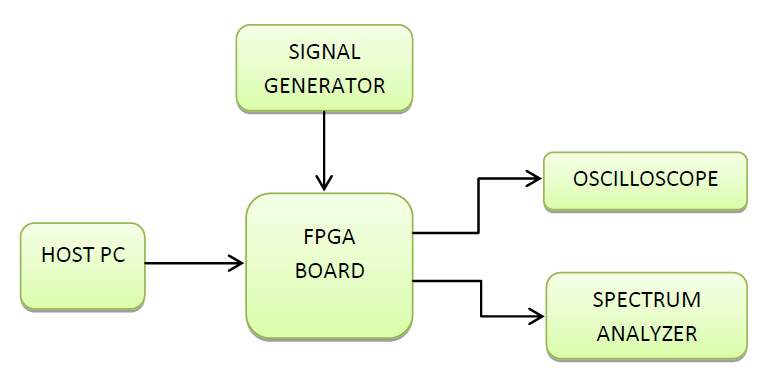
Figure 50: Block Diagram for Design Verification
FPGA Board
The FPGA board used in our project is a VC707 Evaluation Board with Virtex-7 FPGA XC7VX485T-2FFG1761C.
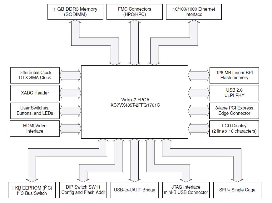
Figure 51: VC707 Board Block Diagram[19]
Key Features:
- FPGA: Virtex XC7VX485T-2FFG1761C
- 128MB (1024Mb) Linear BPI Flash for PCIe Configuration
- 16MB (128Mb) Quad SPI Flash
- 1GB DDR3 SODIMM 800MHz / 1600Mbps
- Fixed Oscillator with differential 200MHz output: System Clock
- Programmable Oscillator with 156.250 MHz as the default output
- 12V wall adapter or ATX
Refer Appendix for All Board Features.
Host PC
The host PC can be any general purpose system installed with the FPGA platform, in this project it is Vivado 2015.1. All the interfacing files required for clocking the FPGA, initializing the ADCs and DACs of the FPGA, VHDL code of the developed model should be present here. The following steps need to be followed to initialize the FPGA and verify the model.
- Open vivado 2015.1.
- Select card control and the open card.
- In the interface select PCI and for card type choose Benone PCI.
- Right click on virtex 2 assign and configure select the location of bit file for clock
- Right click on virtex 4 assign and configure select the location of bit file for ADC
- Right click on virtex 2 assign and configure select location of bit file of designed model.
Signal Generator
Signal generator is used to synthesize both message and carrier signals for the system model ported onto the FPGA. The signal generator used here can generator 9 KHz to 18 GHz signal. The output of signal generator is given to the ADC IP on the FPGA.
Spectrum Analyzer
Spectrum Analyzer is used to display the spectrum of the required signal. The output from the DAC on FPGA is connected to spectrum analyzer input to verify the modulating signal.
Oscilloscope
Oscilloscope is used to display the signal in time domain. The output from DAC of FPGA is connected to oscilloscope input to verify the modulating signal.
11 Vivado’s Xilinx Design Suite
We used Vivado’s Xilinx Design Suite Version 2015.1 for the project. It was used for testing and verification of the Monitoring Receiver Model that was developed. Figures 52 to 58 show the view of the model as seen in the Design Suite.
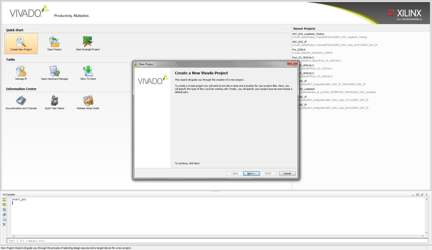
Figure 52: Starting Page for creating a project
The next option has to be clicked to continue and required parameters need to be filled in the dialogue boxes that open. The steps to create a project are given below in brief:
- Click on create project -> next
- Give a Name for the project and select location -> next
- Select Project type (RTL) -> next -> next
- Select the hardware for your project from the list -> next -> finish
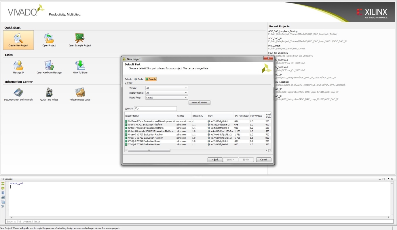
Figure 53: Select Virtex 7 VC707 evaluation Board Platform 1.1
The next step is Synthesis; then we add IP or User constraint file. We have added IP for the ADC card in our model. The IP for monitoring receiver is generated and gets added in the model. The hardware is configured and Implementation is complete which generated the bit file. This Bit file is used to programme the FPGA after which the performance can be measured on an Oscilloscope.
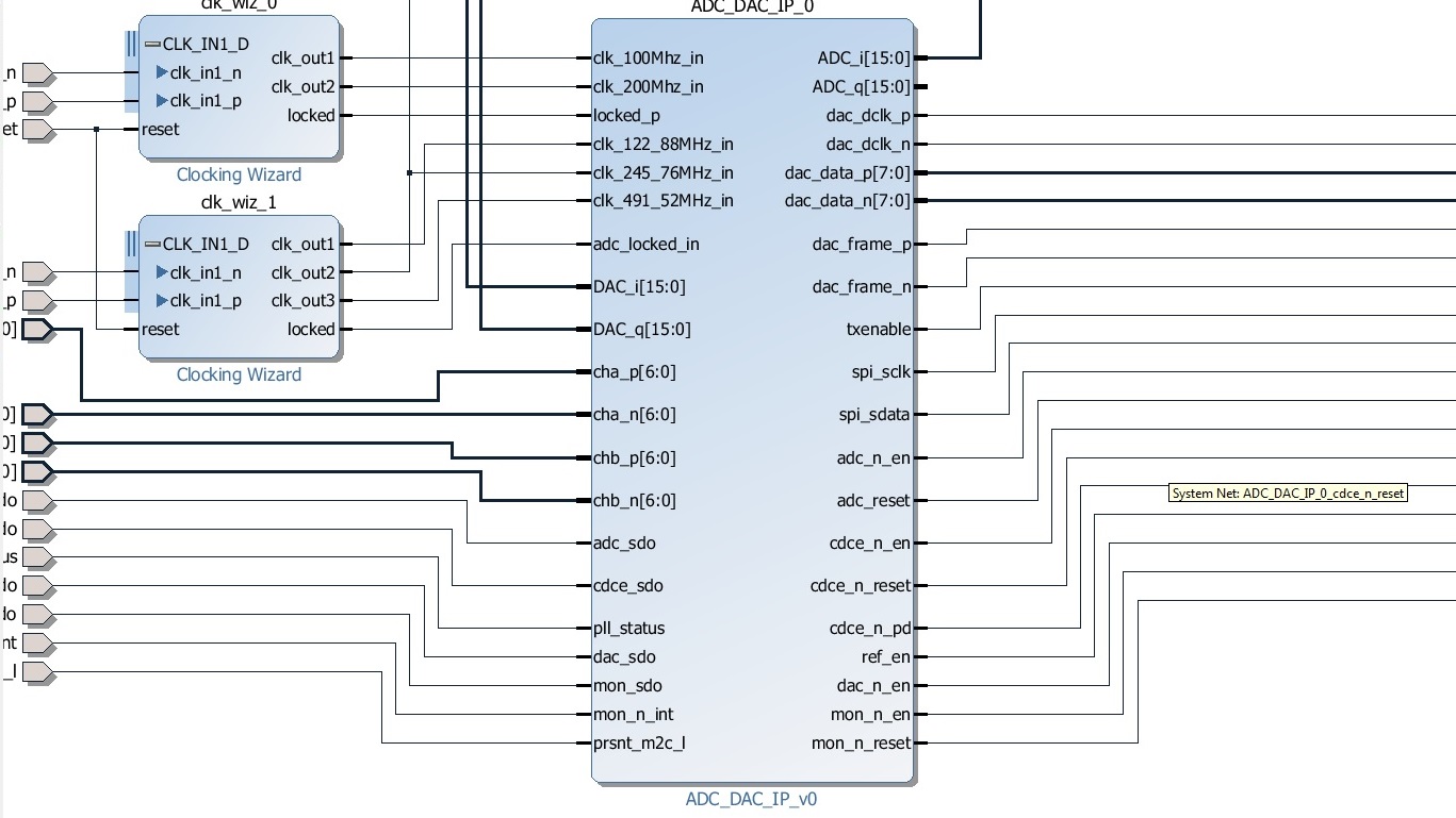
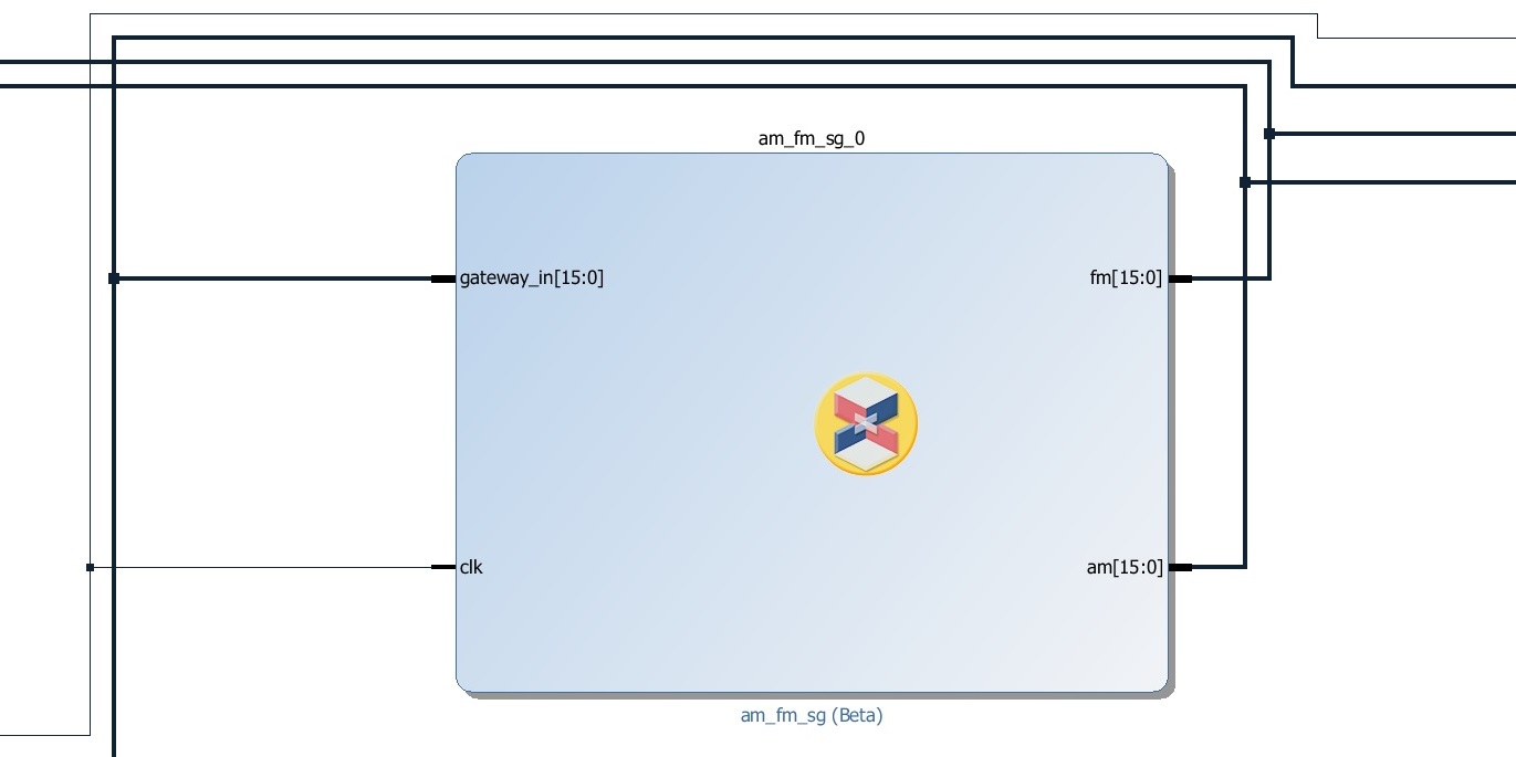
Figure 55: Monitoring Receiver IP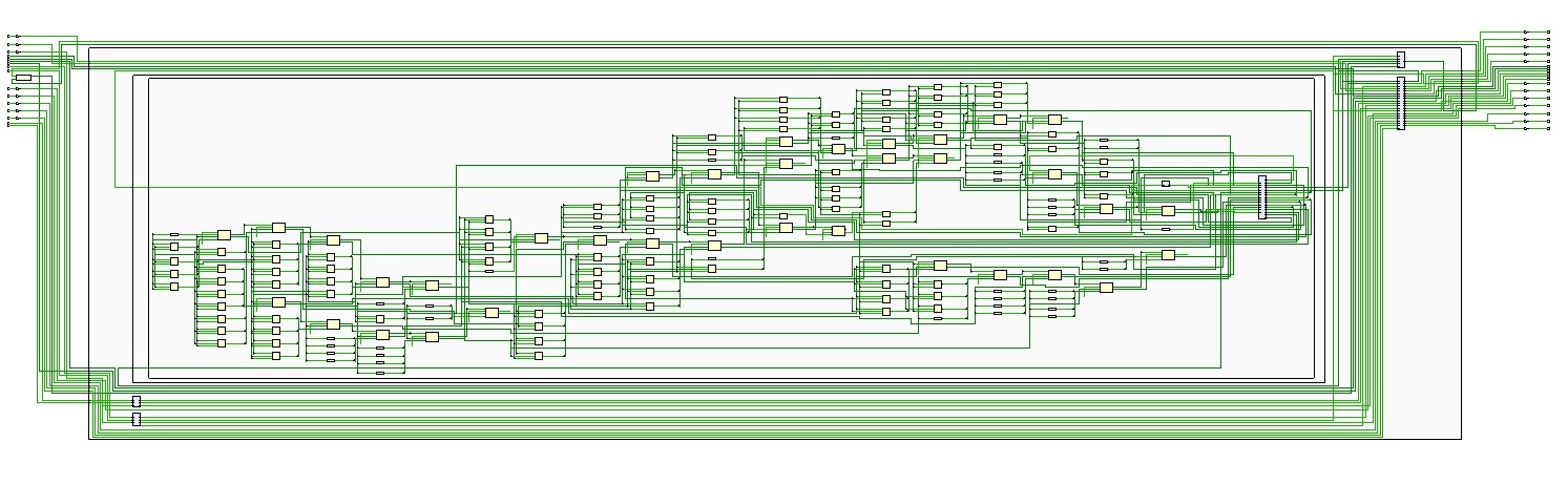
Figure 56: LUTs of FPGA used for Monitoring Receiver
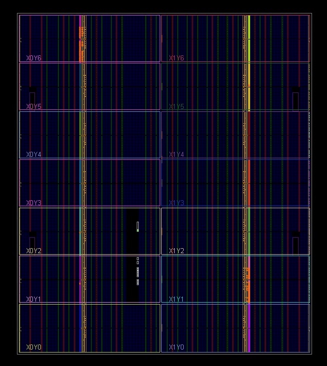
Figure 57: Area occupied by monitoring receiver in Sectors of FPGA
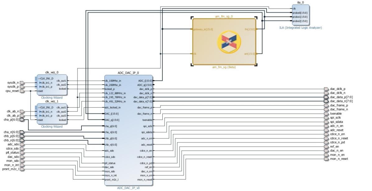
Figure 58: Block view of the Project
12 Results
Observed on Time Scope
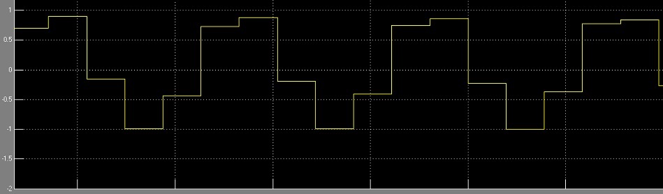
Figure 59: Sine Wave Output from DDS
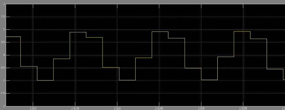
Figure 60: Cosine Wave Output from DDS
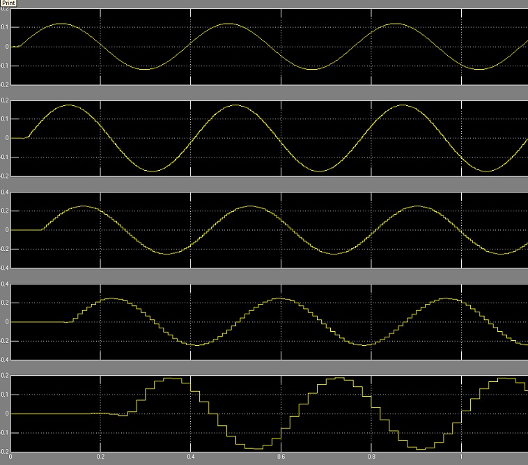
Figure 61: Output on Selection of Different Sampling Rate: a) 800KHz b)400KHz c)200KHz d) 100KHz e)50KHz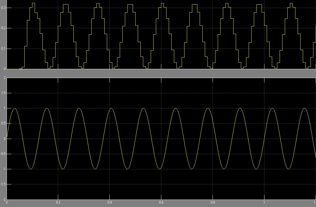
Figure 62: AM: a) Demodulated wave b) Modulated Wave
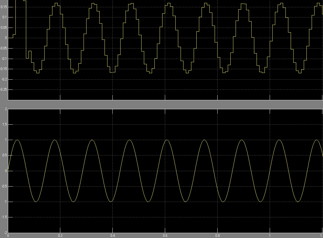
Figure 63: FM: a) Demodulated Wave b) Modulated Wave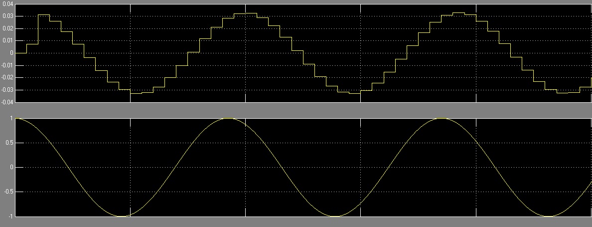
Figure 64: DSB-SC: a) Demodulated Wave b) Modulated Wave
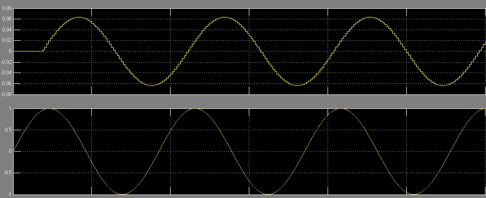
Figure 65: SSB: a) Demodulated Wave b) Modulated Wave
Observed on Spectrum Scope
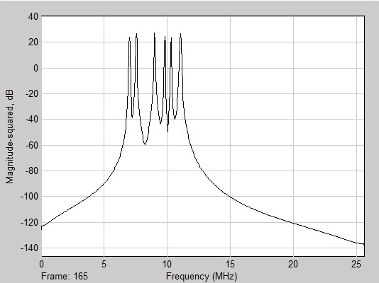
Figure 66: Spectrum of Band Pass Input: Peak at 10.7MHz (IF) will be kept and rest will get filtered out.
Observed on CRO
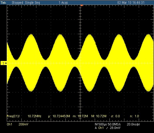
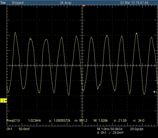
Figure 68: AM Demodulated Wave
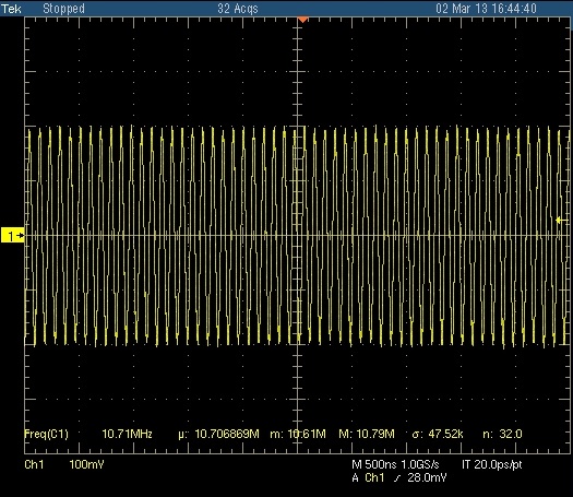
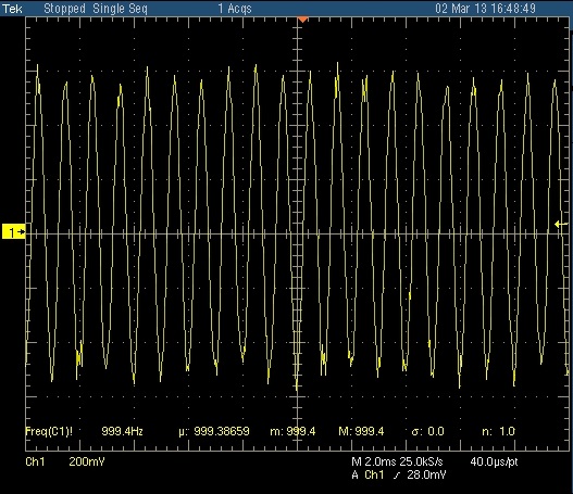
Figure 70: FM Demodulated Wave
13. Conclusion
Sensitivity
The SINAD values inferred from the results are:
DSB-AM: 10dB
DSB-SC AM: 11dB
SSB: 13dB
FM: 19dB
The SINAD value received at 0dBm is 50dB. From the values, we infer that we cannot input a signal below -65dBm, else we will not be able to receive all the signals and they will become non-recoverable.
Dynamic Range
Maximum Value = 0dB and Minimum Value = -65dB. Therefore, the dynamic range of the system is found to be 65dB.
Maximum Input Level
The maximum input level is 0dBm.
Resource Used
The design occupies approximately 2% of the hardware. This can be seen from the Utilization Report Clearly.
| Site Type | Used | Fixed | Available | Utilization % |
| Slice LUTs | 8949 | 0 | 303600 | 2.95 |
| LUT as Logic | 4866 | 0 | 303600 | 1.60 |
| LUT as Memory | 4083 | 0 | 130800 | 3.12 |
| LUT as Distributed RAM | 24 | 0 | ||
| Slice Registers | 11841 | 0 | 607200 | 1.95 |
| Registers as Flip Flop | 11841 | 0 | 607200 | 1.95 |
| Register as Latch | 0 | 0 | 607200 | 0.00 |
| F7 Muxes | 30 | 0 | 151800 | 0.02 |
| F8 Muxes | 4 | 0 | 75900 | <0.01 |
Refer to Appendix for the complete Utilization Report.
14. Future Scope
The first phase of the project has been completed with satisfactory results. Using various analog demodulation techniques, we have achieved appropriate values of SINAD for the proper functioning of Monitoring Receiver.
An Automatic Gain Control (AGC) circuit can be added as an additional block in the design. This will help in keeping the receiver’s output level from fluctuating too much by detecting the overall strength of the signal and automatically adjusting the gain of the receiver to maintain the output level within an acceptable range. It will also help in prevention of overload on strong signals.
An advanced version of the receiver can be made using digital demodulation techniques like PSK, FSK, QPSK, ASK etc. Signal Processing and analysis can be made digital too. This will increase the versatility of the receiver.
15. Bibliography
- https://en.wikipedia.org/wiki/Virtex_(FPGA)
- https://en.wikipedia.org/wiki/Xilinx
- Lyons, R. (2000). Quadrature signals: complex, but not complicated. URL: http://www. dspguru. com/info/tutor/quadsig. htm.
- http://allaboutfpga.com/fpga-design-flow/
- 7 Series FPGAs Configuration User Guide www.xilinx.com 61 UG470 (v1.10) June 24, 2015
- Adamy, D. L. (2008). EW 103: Tactical battlefield communications electronic warfare. Artech House.
- Kuon, I., Tessier, R., & Rose, J. (2008). FPGA architecture: Survey and challenges. Foundations and Trends in Electronic Design Automation, 2(2), 135-253.
- Woods, R., McAllister, J., Lightbody, G., & Yi, Y. (2008). Front Matter (pp. i-xxi). John Wiley & Sons, Ltd.
- Trimberger, S. M. (Ed.). (2012). Field-programmable gate array technology. Springer Science & Business Media.
- Hosking, R. H. H. (1998). Software Defined R ware Defined R ware Defined Radio Handbook adio Handbook.
- Stine, J. E. (2012). Digital computer arithmetic datapath design using verilog HDL. Springer Science & Business Media.
- http://www.people.vcu.edu/~rhklenke/tutorials/actel/design_flow.html
- Hollis, T., & Weir, R. (2003). The theory of digital down conversion. Hunt Engineering.
- www.ics.uci.edu/~magda/Courses/netsys270/ch4_2_v1.ppt
- Semiconductor, L. (2007). THE FPGA AS A FLEXIBLE AND LOW-COST DIGITAL SOLUTION FOR WIRELESS BASE STATIONS.
- DS180 (v1.17) May 27, 2015 www.xilinx.com, Product Specification
- Alter, J. J., & Coleman, J. O. (2008). Radar Digital Signal Processing. Radar Handbook (Merrill Skolnik ed.) ch, 25, 25-1.
- http://ece.gmu.edu/coursewebpages/ECE/ECE545/F10/viewgraphs/ECE545_lecture9_FPGAs_6.pdf
- Shima, J. M. (1995). FM demodulation using a digital radio and digital signal processing (Doctoral dissertation, University of Florida).
- Burnett, N. (2010). FM Radio Receiver with Digital Demodulation (Doctoral dissertation, California Polytechnic State University, San Luis Obispo).
- http://www.xilinx.com/itp/xilinx10/isehelp/ise_c_advanced_flow.htm
- http://www.xilinx.com/itp/xilinx10/isehelp/ise_c_advanced_flow_overview.htm
- www.chipdesigncollege.com/Files/mavo/FPGA_ASIC_Technologies_Flow.pdf
- Schnyder, F., & Haller, C. (2002). Implementation of FM demodulator algorithms on a high performance digital signal processor. Nanyang Technological University and Hochschule For Technik Rapperswil, Tech. Rep.
- http://www.eecs.wsu.edu/~ee314/handouts/numsys.pdf
- http://www.ncert.nic.in/ncerts/l/iemh101.pdf
- Lyons, R. (2000). Quadrature signals: complex, but not complicated. URL: http://www. dspguru. com/info/tutor/quadsig. htm.
- https://rutherglen.science.mq.edu.au/wchen/lnfycfolder/fyc01.pdf
- http://www.denisowski.org/Articles/Denisowski%20%20Spectrum%20Anlyzers%20vs.%20Monitoring%20Receivers.pdf
- System Generator for DSP Getting Started Guide www.xilinx.com UG639 (v 14.3) October 16, 2012
- System Generator for DSP Getting Started Guide www.xilinx.com UG639 (v11.4) December 2, 2009
- Vivado: Designing with System Generator www.xilinx.comUG897 (v2016.2) June 8, 2016
- VC707 Evaluation Board www.xilinx.com UG885 (v1.2) February 1, 2013
- UG470 (v1.10) June 24, 2015 www.xilinx.com 7 Series FPGAs Configuration User Guide
Appendix
- VC707 Board Features
• Virtex-7 XC7VX485T-2FFG1761C FPGA
• 1 GB DDR3 memory SODIMM
• 128 MB Linear byte peripheral interface (BPI) Flash memory
• USB 2.0 ULPI Transceiver
• Secure Digital (SD) connector
• USB JTAG through Digilent module
• Clock Generation
• Fixed 200 MHz LVDS oscillator (differential)
• I2C programmable LVDS oscillator (differential)
• SMA connectors (differential)
• SMA connectors for GTX transceiver clocking
• GTX transceivers
• FMC1 HPC connector (eight GTX transceivers)
• FMC2 HPC connector (eight GTX transceiver)
• SMA connectors (one pair each for TX, RX and REFCLK)
• PCI Express (eight lanes)
• Small form-factor pluggable plus (SFP+) connector
• Ethernet PHY SGMII interface (RJ-45 connector)
• PCI Express endpoint connectivity
• Gen1 8-lane (x8)
• Gen2 8-lane (x8)
• SFP+ Connector
• 10/100/1000 tri-speed Ethernet PHY
• USB-to-UART bridge
• HDMI codec
• I2C bus
• I2C MUX
• I2C EEPROM (1 KB)
• USER I2C programmable LVDS oscillator
• DDR3 SODIMM socket
• HDMI codec
• FMC1 HPC connector
• FMC2 HPC connector
• SFP+ connector
• I2C programmable jitter-attenuating precision clock multiplier
• Status LEDs
• Ethernet status
• Power good
• FPGA INIT
• FPGA DONE
• User I/O
• User LEDs (eight GPIO)
• User pushbuttons (five directional)
• CPU reset pushbutton
• User DIP switch (8-pole GPIO)
• User SMA GPIO connectors (one pair)
• LCD character display (16 characters x 2 lines)
• Switches
• Power on/off slide switch
• FPGA_PROB_B pushbutton
• Configuration mode DIP switch
• VITA 57.1 FMC1 HPC Connector
• VITA 57.1 FMC2 HPC Connector
• Power management
• PMBus voltage and current monitoring through TI power controller
• XADC header
• Configuration options
• Linear BPI Flash memory
• USB JTAG configuration port
• Platform cable header JTAG configuration port
- Communication & Networking
- Gigabit Ethernet GMII, RGMII and SGMII
- SFP+ transceiver connector
- GTX port (TX, RX) with four SMA connectors
- UART To USB Bridge
- PCI Express x8 gen2 Edge Connector (lay out for Gen3)
- Display
- HDMI Video OUT
- 2 x16 LCD display
- 8X LEDs
- Expansion Connectors
- FMC1 – HPC (8 XCVR, 160 single ended or 80 differential (34 LA pairs, 24 HA pairs, 22 HB pairs) user-defined pins)
- FMC2 – HPC (8 XCVR, 116 single ended or 58 differential (34 LA pairs, 24 HA pairs) user-defined pins)
- Vadj supports 1.8V
- IIC
- SINAD
Signal-to-noise and distortion ratio (SINAD) is a measure of the quality of a signal from a communications device, often defined as:
SINAD= Psignal+Pnoise+PdistortionPnoise+Pdistortion
Where,
Pis the average power of the signal, SINAD is usually expressed in dB and is provided alongside the receiver RF sensitivity, to give a quantitative evaluation of the receiver sensitivity. Unlike SNR(may or may not be less than 1), SINAD reading can never be less than 1 (i.e. it is always positive when quoted in dB).
A lower SINAD value implies worse performance of the system. As the got RF flag ends up it appears that evidently weaker it seems to be logically misplaced within the commotion and mutilation created via collector, demodulation and sound yield drive circuits.
- Automatic Gain Control
AGC is a closed loop feedback directing circuit which gives controlled flag adequacy at its yield, in spite of the variety of abundancy in information input flag. The normal or peak yield flag(signal) level is utilized to progressively modify the contribution to-yield pick up to a satisfactorily to a greater range, empowering the circuit to work attractively with a more prominent scope of input level signals. It is used in most radio receivers to equalize the average volume (loudness) of different radio stations due to differences in received signal strength, as well as variations in a single station’s radio signal due to fading. For a very weak signal, the AGC operates the receiver at maximum gain; as the signal increases, the AGC reduces the gain.
[1] Adamy, D. L. (2000). EW 101. Artech House.
[2] FM3.36, op.cit. 15
[3] Kuon, I., Tessier, R., & Rose, J. (2008). FPGA architecture: Survey and challenges. Foundations and Trends in Electronic Design Automation, 2(2), 135-253.
[4] https://en.wikipedia.org/wiki/Field-programmable_gate_array
[5] Hosking, R. H. H. (1998). Software Defined Radio Handbook, Pentek Inc.
[6] http://www.gensys.co.in/project5.html
[7] https://www.xilinx.com/products/boards-and-kits/ek-v7-vc707-g.html
[8]http://www.robkalmeijer.nl/techniek/electronica/radiotechniek/hambladen/qex/2002/07_08/page44/ index.html
[9] www.xilinx.com System Generator for DSP Getting Started Guide UG639 (v 14.3) October 16, 2012
[10] Haykin, S. (2008). Communication systems. John Wiley & Sons.
[11] https://en.wikipedia.org/wiki/Amplitude_modulation, accessed on Aug 01, 2016
[12] https://en.wikipedia.org/wiki/Sideband
[13] https://en.wikipedia.org/wiki/Amplitude_modulation
[14] https://en.wikipedia.org/wiki/Double-sideband_suppressed-carrier_transmission
[15] Wright, H. (2000). Testing digital communications transmitters and receivers. Microwave Journal, 43(7), 136-136.
[16] https://en.wikipedia.org/wiki/Antenna_(radio)
[17] https://en.wikipedia.org/wiki/Tuner_(radio)
[18] http://www.xilinx.com/itp/xilinx10/isehelp/ise_c_fpga_design_flow_overview.htm
Y [19] VC707 Evaluation Board, www.xilinx.com, UG885 (v1.2) February 1, 2013
Cite This Work
To export a reference to this article please select a referencing stye below:
Related Services
View all


Related Content
All TagsContent relating to: "Computer Science"
Computer science is the study of computer systems, computing technologies, data, data structures and algorithms. Computer science provides essential skills and knowledge for a wide range of computing and computer-related professions.
Related Articles

DMCA / Removal Request
If you are the original writer of this dissertation and no longer wish to have your work published on the UKDiss.com website then please: