High Resistivity Silicon: Deep-Level Doping Compensation Using Elemental Gold
Info: 4120 words (16 pages) Dissertation
Published: 16th Dec 2019
Tagged: Sciences
High Resistivity Silicon: Deep-Level Doping Compensation Using Elemental Gold
Abstract—The potential of using transition elements as deep level dopants for n-type Czochralski silicon (Cz-Si) substrate has been investigated. The resistivity enhancement of n-type Si substrate provided by studied transition elements, i.e. gold (Au), silver (Ag), cobalt (Co), palladium (Pd), vanadium (V), manganese (Mn) and platinum (Pt) was determined and analyzed. It is shown that Au and Ag are the most suitable elements to be used as deep level dopants for n-type Si substrate. Au is better suited for the goal as it is more well-studied as compared to Ag. The use of Co and Pd are not desirable due to requirement of high solubility. V, Mn and Pt are disqualified as they do not provide compensation for n-type Si substrate. There is a significant difference between the results of theoretical calculation and measurement made on actual n-type Au-compensated Cz-Si wafer due to the existence of inactive surface Au layer on Si wafer.
IndexTerms—Czochralski silicon, deep level dopant, gold, high resistivity silicon, resistivity enhancement
I. Introduction
High resistivity silicon substrate is important to improve signal isolation and minimize substrate cross-talk in radio frequency (RF) and analog/mixed signal (AMS) integrated circuit application [1]. The commercially available float-zone (FZ) silicon growth technology offers a solution with resistivity up to 70 kΩ-cm [2]. However, its maximum wafer diameter is limited to 8’’ and thus not suitable for modern CMOS processing where the standard wafer diameter is 12’’. Silicon-on-insulator (SOI) and silicon-on-anything (SOA) technologies have been proposed as alternative solutions for this problem [3]. Nonetheless, thermal breakdown issue occurs on SOI and SOA wafers due to on-chip heat dissipation problem [4]. Hence, there is a need to increase the bulk resistivity of Czochralski silicon (Cz-Si) substrate as a low-cost solution, by reducing the background free carrier concentration which is inversely proportional to substrate resistivity.
In this work, a concept called deep level doping compensation technique is studied. The doping of deep impurities into Cz-Si substrate introduces deep levels which pin the Fermi level near the middle of Si bandgap [5]. Hence, semi-insulating Si substrate is produced using this technique. The main objective of this work is to investigate the potential of using transition elements as deep level dopant for n-type Cz-Si substrate. The resistivity enhancement of n-type Si compensated with studied transition elements, i.e. gold (Au), silver (Ag), cobalt (Co), palladium (Pd), vanadium (V), manganese (Mn) and platinum (Pt) was evaluated to assess their suitability.
II. Related work
This work is inspired by that of Mallik et al. [6], who analysed the possibility of using deep level impurities in producing high resistivity p-type Cz-Si substrate. They theoretically show that the transition elements are suitable candidates for deep level doping compensation technique. However, this study differs from Mallik et al. in one important respect: n-type Cz-Si is used for the analysis rather than p-type Cz-Si.
A follow-up study by Mallik et al. [7] has been conducted on fabrication of high resistivity p-type Cz-Si substrate using deep level Mn doping. The drawback of this approach is that Mn concentration is required to be tightly controlled to maximize resistivity enhancement. Jordan et al. [8] use Au as deep level dopant for both p-type and n-type Cz-Si substrate. They show that n-type substrate achieves a higher resistivity as compared to p-type substrate. However, the potential of using transition elements rather than Au as deep level dopants for n-type Cz-Si substrate has not been discussed by the works mentioned in this section.
III. Methodology
The resistivity of n-type Cz-Si compensated using studied transition elements can be determined through the methods used by Mallik et al. [6]. The Fermi level
EFwas determined by solving the charge neutrality equation given by:
| p+∑iNDi+-n-∑jNAj-=0 | (1) |
In (1),
nand
pare the free hole and electron concentrations given by:
| n=NC e-(EC-EF)/kT | (2) | |
| p=NV e-(EF-EV)/kT | (3) |
where
kis the Boltzmann constant, and
Tis taken as 300 K.
NCand
NVare the temperature-dependent effective densities of states of the conduction (
EC) and valence (
EV) bands respectively. The values of
NCand
NVare taken as 2.8 x 1019 cm-3 and 1.04 x 1019 cm-3 respectively at 300 K [9].
The
NDi+and
NAj-are the ith and jth ionised donor and acceptor concentration for a total impurity density of
NDiand
NAjrespectively. For shallow impurities, such as boron and phosphorus which only contributes single donor or acceptor level, the expression for
NDi+and
NAj-are given by [10]:
TABLE I POSITIONS OF ENERGY LEVELS OF TRANSITION ELEMENTS IN SILICON[11]
| Element | Donor level below EC (eV) | Acceptor level above EV (eV) |
| Co | 0.89 | 0.82 |
| Pd | 0.84 | 0.9 |
| Au | 0.78 | 0.56 |
| Ag | 0.75 | 0.545 |
| V | 0.45 | 0.92 |
| Mn | 0.42 | 1.0 |
| Pt | 0.314 | 0.889 |
TABLE II Parameters used in equations (8) and (9) for hole and electron mobilities [13], [14]
| Parameter | Hole | Electron |
| μ0 | 473 cm2/V s | 1448 cm2/V s |
| T0 | 300 K | 300 K |
| A | 1.0×10¹⁷/cm/V/s/K3/2 | 4.61×10¹⁷/cm/V/s/K3/2 |
| B | 6.25×10¹⁴/cm3/K2 | 1.52×10¹⁵/cm3/K2 |
| Nscat | ∑iNDi++∑jNAj- | ∑iNDi++∑jNAj- |
| Ncar | ∑jNAj–∑iNDi+ | ∑iNDi+-∑jNAj- |
| NDi+=NDi(1+gi eEF-EDikT)-1 | (4) | |
| NAj-=NAj(1+gj eEAj-EFkT)-1 | (5) |
where
EDi(
EAj) is the energy position of the ith (jth) impurity level, measured from the valence band for a donor (acceptor), gi and gj are the corresponding degeneracy of donor and acceptor impurity. It is assumed that deep level dopants only create a pair of donor (
ED) and acceptor (
EA) levels in Si bandgap, which are shown in Table I [11]. Therefore, the ionised concentration of deep donors and acceptors are given by [12]:
| ND+=ND(1+gD eEF-EDkT+e2EF-EA-EDkT)-1 | (6) | |
| NA-=NA(1+gA eEA-EFkT+eEA+ED-2EFkT)-1 | (7) |
For n-type Cz-Si substrate, the total ionised donor concentration is the sum of ionised donor concentrations of phosphorus and deep dopants calculated using (4) and (6). The energy position of phosphorus donor was taken as EC – 0.045 eV, and degeneracy (
g) for donor and acceptor are 2 and 4 respectively. The charge neutrality equation was solved numerically to obtain the Fermi level
EF.
Then, the values of free hole (n) and electron (p) concentrations were calculated by substituting the values of EF obtained from numerical solution. The total ionised deep donor (
ND+) and acceptor (
NA-) concentrations were calculated for deep dopant density ranged from 1013 cm-3 to 1018 cm-3.
The hole (
μp) and electron (
μn) mobilities are required in the calculation of the resistivity of Si. The mobilities of the holes and electrons are limited by lattice scattering and the active impurities scattering mechanisms. The expression for mobilities limited by both mechanisms are given by [13], [14]:
| μlattice=μ0 (TT0)-α | (8) |
| μimpurities=AT32Nscatln1+BT2Ncar-BT2Ncar+BT2-1 | (9) |
where
Nscatrepresents the number of scattering sites introduced by impurities and
Ncarrepresents the number of free carriers available for screening. The parameters used in (8) and (9) for hole and electron mobilities are shown in Table II.
However, an assumption was made that the mobility due to impurity scattering,
μimpuritiesis removed from the calculation when
Ncarhas a zero or negative value, i.e. the mobility of carriers is solely limited by lattice scattering. Both hole and electron mobilities due to both mechanisms were combined using Matthiessen’s rule given by [15]:
| 1μ=1μlattice+1μimpurities | (10) |
The obtained values for free hole and electrons concentrations (
nand
p) and mobilities (
μpand
μn) were used for the calculation of resistivity of n-type Si which is given by:
| ρ=1qnμn+pμp | (11) |
where
qis the electronic charge given by 1.6 x 10⁻¹⁹ C.
IV. Results and discussion
The resistivity of n-type Cz-Si doped with studied transition elements, i.e. Au, Ag, Co, Pd, V, Mn and Pt were calculated for the deep dopant densities ranging from 1013 to 1018 cm-3. Fig. 1 illustrates the resistivity of Si substrate with a background phosphorus concentration of 1014 cm-3 compensated using studied transition elements. It is observed that the resistivity of n-type Si substrate increases with the addition of deep dopant Au, Ag, Co and Pd. The resistivity plots for Au and Ag are almost similar since their deep donor and acceptor levels are very close to each other. The resistivity of n-type Si doped with Au or Ag initially increases from about 50 Ω-cm until a peak is reached which is about 5×10⁵ Ω-cm. The resistivity of n-type Si subsequently decreases with further addition of deep dopant Au and Ag until it settles at a resistivity of about 105 Ω-cm. The enhancement of resistivity is about four orders of magnitude. Au and Ag are the most suitable elements for deep level doping compensation since both elements have deep donor and acceptor levels nearest to the middle of Si bandgap. The results for Au are consistent with theoretical calculation made by Jordan et al. [8]. However, Ag has the disadvantage of being comparatively less well-studied.
(a)
(b)
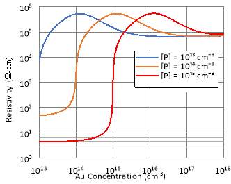
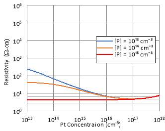
Fig. 2. Calculated resistivity of Si at 300 K as a function of (a) Au and (b) Pt concentrations for three different background phosphorus concentrations in cm-3.
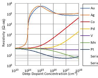
Fig. 1. Calculated resistivity of Si at 300 K as a function of deep dopant concentrations of studied transition elements for background phosphorus concentration of 1014 cm-3.
Meanwhile, it is observed that the resistivity of n-type Si increases sub-linearly with the increase in concentration of Co and Pd. The starting resistivity of n-type Si doped with Co or Pd are the same, which is about 40 Ω-cm. The Co-compensated n-type Si substrate achieves a higher resistivity as compared to Pd-compensated n-type Si substrate since the deep acceptor level of Co is nearer to the intrinsic Fermi level of Si. The final resistivity of n-type Si at deep dopant densities of 1018 cm-3 are 4×10⁴ Ω-cm for Co and 2×103 cm-3 for Pd. Co and Pd still provide compensation for n-type Cz-Si as their deep donor and acceptor levels are considerably near the intrinsic Fermi level of Si. The disadvantage of using Co and Pd as deep level dopants is that higher doses of Co and Pd are required to produce n-type Si substrate with resistivity over 1 kΩ-cm as compared to Au-compensated and Ag-compensated n-type Si substrate. This can only occur when the solubilities of Co and Pd in Si are high.
However, V, Mn and Pt do not provide required compensation to increase the resistivity of n-type Si. The starting resistivity of n-type Si compensated with these three elements are low, which is at 40 Ω-cm. The resistivity of n-type Si generally decreases with the increase in the concentrations of V, Mn and Pt. The deep donor levels of these three elements are near the conduction band. Hence, more ionised electrons are contributed from these three elements to the conduction band. The holes attracted to the deep acceptor levels of these three elements are not sufficient to compensate for the ionised electrons from the conduction band.
In sum, Au and Ag are the most suitable transition elements as deep level dopants for n-type Cz-Si. On the other hand, Pt are considered as the worst elements among the transition elements which do not provide compensation for n-type Si since it has the deep donor level nearest to conduction band. Further analysis was made for both Au and Pt by varying the background phosphorus concentration of Si substrate. Fig. 2 illustrates the resistivity of Si substrate with three different background phosphorus concentrations compensated with Au and Pt respectively.
It is shown in fig. 2(a) that Au provides compensation for n-type Si doped with background phosphorus concentrations of 1013, 1014 and 1015 cm-3 in a similar manner. The resistivity of n-type Si initially increases with the addition of deep dopant Au until a maximum value is reached. The initial resistivity is low due to under-compensation caused by insufficient number of deep dopant Au. The peak in resistivity of n-type Si is reached when deep dopant Au exactly compensates for the phosphorus donors. Further increase in Au concentration causes overcompensation, rendering the substrate into p-type. This results in a fall of resistivity of Si substrate.
Pt does not provide any compensation for n-type Si with varying background phosphorus concentrations as shown in fig. 2(b). The highest resistivity of Pt-compensated Si substrate observed is the starting resistivity with a background phosphorus concentration of 1013 cm-3, which is about 250 Ω-cm. Therefore, this substrate is not suitable for RF-MMIC application since a substrate of resistivity of at least 3 kΩ-cm is required for low CPW loss [16], [17].
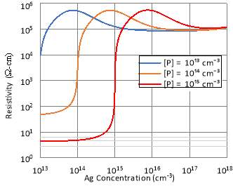
Fig. 3. Calculated resistivity of Si at 300 K as a function of Ag concentration for three different background phosphorus concentrations in cm-3.
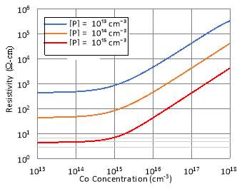
Fig. 4. Calculated resistivity of Si at 300 K as a function of Co concentration for three different background phosphorus concentrations in cm-3.
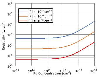
Fig. 5. Calculated resistivity of Si at 300 K as a function of Pd concentration for three different background phosphorus concentrations in cm-3.
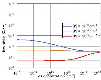
Fig. 6. Calculated resistivity of Si at 300 K as a function of V concentration for three different background phosphorus concentrations in cm-3.
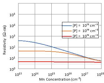
Fig. 7. Calculated resistivity of Si at 300 K as a function of Mn concentration for three different background phosphorus concentrations in cm-3.
The resistivity plots of n-type Cz-Si substrate compensated using other studied transition elements rather than Au and Pt are shown in fig. 3 to fig. 7. The nature of deep level doping compensation from the studied transition elements generally does not change with varying background phosphorus concentration. The increase in background phosphorus concentration only increases the required deep dopant density to compensate for free carrier donors contributed by phosphorus for the case of Au, Ag, Co and Pd.
The comparison was made between the results of theoretical calculation in this work and the published data from Hashim [18]. The 6-inch, Phosphorus-doped, n-type <100> Czochralski-grown Si wafers used in Hashim’s work have an average wafer thickness of 675 µm with nominal resistivity ranging between 50 Ω-cm and 60 Ω-cm. The wafers were implanted with an energy of 100 keV and an implantation dose of 4 x 1013 cm-2, which corresponds to Au concentration of approximately 8 x 1014 cm-3. The maximum resistivity recorded among the wafers are 80 kΩ-cm.
Fig. 8 illustrates the theoretical calculation and experimental results for the resistivity of n-type Au-compensated Cz-Si. The theoretical resistivity of the Si wafer with Au dopant concentration of 8 x 1014 cm-3 was calculated using the methods discussed in Section III by varying phosphorus concentration between 1013 cm-3 and 1015 cm-3. The initial starting resistivity was taken as 50 Ω-cm, which corresponds to background phosphorus concentration of approximately 8.6 x 1013 cm-3. The theoretical resistivity of Au-compensated Cz-Si doped with this phosphorus concentration is about 500 kΩ-cm. The experimental result is lower than expected because the actual Au concentration in the wafer is lower than the implanted Au concentration. A thin electrically inactive Au layers exists on the wafer surfaces which does not compensate for free carriers in the Si wafer. The existence of this inactive surface Au layer has been proven with the finding in [19]. However, the experimental result shows that Au dopant can be used to produce high resistivity n-type Cz-Si with a resistivity enhancement of about three orders of magnitude.
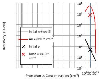
Fig. 8. Theoretical and experimental results for resistivity of Si with and without Au dopant. Crosses and curves are measured [18] and calculated values respectively.
V. Conclusion
The potential of using transition elements as deep level dopants for n-type Cz-Si was demonstrated in this work. It is found that Au and Ag are most suitable to be used for deep level doping compensation as they have their deep donor and acceptors near intrinsic Fermi level of Si. The theoretical resistivity enhancement of n-type Cz-Si substrate provided by these two elements are about four orders of magnitude. Au is better suited for the goal as it is more well-studied as compared to Ag.
Acknowledgment
The author would like to thank Dr. Nur Zatil ‘Ismah Hashim and Dr. Mohamad Adzhar Md Zawawi for useful discussions.
References
[1] “RF and AMS tech for wireless communications,” International Technology Roadmap for Semiconductors, 2009. [Online]. Available: http://www.itrs2.net/itrs-reports.html. [Accessed: 28-Feb-2017].
[2] “High resistivity silicon for GHz and THz technology,” Topsil. [Online]. Available: http://www.topsil.com/en/silicon-products/silicon-wafer-products/hiresTM.aspx. [Accessed: 28-Feb-2017].
[3] R. Dekker, P. G. M. Baltus, and H. G. R. Maas, “Substrate transfer for RF technologies,” IEEE Trans. Electron Devices, vol. 50, no. 3, pp. 747–757, 2003.
[4] N. Nenadovic, V. D’Alessandro, L. K. Nanver, F. Tamigi, N. Rinaldi, and J. W. Slotboom, “A back-wafer contacted silicon-on-glass integrated bipolar process. Part II. A novel analysis of thermal breakdown,” IEEE Trans. Electron Devices, vol. 51, no. 1, pp. 51–62, 2004.
[5] D. M. Jordan, R. H. Haslam, K. Mallik, and P. R. Wilshaw, “The Development of Semi-Insulating Silicon Substrates for Microwave Devices,” Electrochem. Soc., vol. 16, no. 6, pp. 41–56, 2008.
[6] K. Mallik, R. J. Falster, and P. R. Wilshaw, “‘ Semi-insulating ’ silicon using deep level impurity doping: problems and potential,” Semicond. Sci. Technol., vol. 18, no. 6, p. 517, 2003.
[7] K. Mallik, C. H. De Groot, P. Ashburn, and P. R. Wilshaw, “Enhancement of resistivity of Czochralski silicon by deep level manganese doping,” Appl. Phys. Lett., vol. 89, no. 11, p. 3, 2006.
[8] D. M. Jordan, K. Mallik, R. J. Falster, and P. R. Wilshaw, “Semi-Insulating Silicon for Microwave Devices,” Solid State Phenom., vol. 156–158, pp. 101–106, 2009.
[9] C. C. Hu, “Electrons and Holes in Semiconductors,” in Modern Semiconductor Devices for Integrated Circuits, 1st ed., Upper Saddle River, NJ: Prentice Hall, 2010, p. 21.
[10] A. C. Seabaugh, J. J. Mathias, and M. I. Bell, EPROP: An Interactive FORTRAN Program for Computing Selected Electronic Properties of Gallium Arsenide and Silicon. 1990.
[11] W. Schroeter and M. Seibt, “Deep Levels of Transition Metal Impurities in c-Si,” in Properties of Crystalline Silicon, R. Hull, Ed. London: INSPEC IEE, 1999, p. 561.
[12] A. Milnes, Deep Impurities in Silicon. John Wiley and Sons, 1973.
[13] P. J. Mole, J. M. Rorison, J. A. del Alamo, and D. Lancefield, “Electron mobility, diffusion and lifetime in c-Si,” in Properties of Crystalline Silicon, R. Hull, Ed. New York: INSPEC IEE, 1999, pp. 430–442.
[14] P. J. Mole and J. A. del Alamo, “Hole mobility, diffusion and lifetime in c-Si,” in Properties of Crystalline Silicon, R. Hull, Ed. New York: INSPEC IEE, 1999, pp. 443–449.
[15] S. O. Kasap, “Electrical and Thermal Conduction in Solids,” in Principles of Electronic Materials and Devices, 3rd ed., New York: McGraw-Hill, 2006, p. 127.
[16] W. Heinrich, J. Gerdes, C. Rheinfelder, and K. Strohm, “Coplanar Passive Elements on Si Substrate for Frequencies up to 110 GHz,” IEEE Trans. Microw. Theory Tech., vol. 46, no. 5, pp. 709–712, 1998.
[17] A. C. Reyes, S. M. El-ghazaly, S. J. Dorn, M. Dydyk, D. K. Schroder, and H. Patterson, “Coplanar waveguides and microwave inductors on silicon substrates,” IEEE Trans. Microw. Theory Tech., vol. 43, no. 9, pp. 2016–2022, 1995.
[18] N. Z. I. Hashim, “Au-compensated High Resistivity Silicon for Low Loss Microwave Devices – Suppression of Parasitic Surface Conduction Effect,” Ph.D. dissertation, School of Electron. and Comput. Sci., Univ. Southampton, United Kingdom, 2015.
[19] A. Abuelgasim, “High Resistivity Czochralski-Silicon Using Deep Level Dopant Compensation For RF Passive Devices,” Ph.D. dissertation, School of Electron. and Comput. Sci., Univ. Southampton, United Kingdom, 2012.
Cite This Work
To export a reference to this article please select a referencing stye below:
Related Services
View all


Related Content
All TagsContent relating to: "Sciences"
Sciences covers multiple areas of science, including Biology, Chemistry, Physics, and many other disciplines.
Related Articles

DMCA / Removal Request
If you are the original writer of this dissertation and no longer wish to have your work published on the UKDiss.com website then please: