GSM Innovation for Smart Home Applications
Info: 19820 words (79 pages) Dissertation
Published: 13th Dec 2019
Tagged: BusinessTechnology
List of Figures
| Figure No. | Name of the Figure | Page No. |
| Figure 3.1
Figure 3.2 Figure 4.1 Figure 4.2 Figure 4.3 Figure 4.4 Figure 4.5 Figure 4.6 |
Embedded Layer Architecture
Embedded Architecture Block Diagram Block diagram of Regulated power supply system Transformer circuit Transformer + Rectifier circuit Transformer + Rectifier + Smoothing circuit Transformer + Rectifier + Smoothing + Regulator circuit |
|
| Figure 4.7 | Pin diagram of 8051 Microcontroller | |
| Figure 4.8 | Program Memory of 8051 | |
| Figure 4.9
Figure 4.10 Figure 4.11 |
Latest version of 8051
MAX232 IC MAX232 Pin diagram |
|
| Figure 4.12 | LCD Display | |
| Figure 4.13 | LCD connection | |
| Figure 4.14 | Variable Resistor | |
| Figure 4.15 | Potentiometer symbol | |
| Figure 4.16 | Preset symbol | |
| Figure 4.17 | GSM Module | |
| Figure 4.18 | GSM Module connected to phone | |
| Figure 4.19 | TRIAC symbol and construction | |
| Figure 4.20 | TRIAC I-V characteristic curve | |
| Figure 4.21 | TRAIC Switching circuit | |
| Figure 4.22 | TRAIC Switching circuit 2 | |
| Figure 4.23 | Modified TRAIC Switching circuit | |
| Figure 4.24
Figure 4.25 Figure 4.26 Figure 5.1 |
TRIAC phase control
Circuit symbol of Optocoupler Protecting the LED against reverse voltage ATMEL 8051 Device Programmer |
|
List of Tables
| Table No. | Name of the Table | Page No. |
| Table 1 | List of 8051 Microcontrollers | |
| Table 2 | MAX232 Pins Description | |
| Table 3 | Pins functions of LCD | |
| Table 4 | LCD Commands table | |
| Table 5 | Electrical characteristics | |
| Table 6
Table 7 Table 8 Table 9 Table 10 Table 11 |
Pins and Description of serial port modes
Bud rate calculation for serial port modes List of useful commands for LCD Pin description of MAX232 Voltage levels for MAX232 Electrical Characteristics |
ABSTRACT
The point of this venture is to work different apparatuses at home utilizing SMS from anyplace utilizing portable and this framework additionally screens the heap status and cozy at whatever point it neglects to work. With the present framework we require part of labor to control the switches and more often than not administrator neglects to turn off the lights in the morning which brings about parcel of energy wastage. These issues can be tackled utilizing present innovations. There are numerous innovations turning out to make our lives more agreeable, efficient, more secure and rich. In this venture we are utilizing GSM innovation. Mobile phones utilize GSM innovation. The microcontroller assumes the key part in this venture. The GSM modem will be interfaced to the microcontroller which ceaselessly gets the messages from the client wireless and passes the same to the microcontroller. The GSM modem will be interfaced to the microcontroller area through serial port interface. On the off chance that the client needs to work loads, he can simply send a predefined message to the GSM modem that is interfaced to the controller segment. The controller segment will have the switch controls of the gadgets. Every one of the lights which are to be controlled will be associated with the controlling gadget i.e., to the microcontroller area. The microcontroller consequently, makes an impression on the versatile number about the status of the considerable number of machines. At controlling side we have GSM modem with one SIM, small scale controller, controlling circuit, light status identifying criticism framework. The client needs to send a predefined SMS to the telephone number which embedded in modem then modem will show this new message to ,controller will read this message and control the lights as indicated by message it got. This framework likewise recognizes disappointment condition and shows on power board(LCD) and sends a sms to the client demonstrating the flawed status of fizzled machines.
CHAPTER 1
INTRODUCTION
1.1. INTRODUCTION
The point of this venture is to work the home machines utilizing SMS from anyplace utilizing versatile and this framework likewise screens the light status and private at whatever point it neglects to sparkle.
With the present framework we require parcel of labor to control the switches and more often than not administrator neglects to turn off the lights in the morning which brings about part of energy wastage. These issues can be tackled utilizing present advances. There are numerous advances are turning out to make our lives more solace, efficient, more secure and sumptuous. In this venture we are utilizing GSM innovation.
PDAs utilize GSM innovation. The microcontroller assumes the key part in this venture. The GSM modem will be interfaced to the microcontroller which constantly gets the messages from the client mobile phone and passes the same to the microcontroller.
The GSM modem will be interfaced to the microcontroller segment through serial port interface. On the off chance that the client needs to work the lights, he can simply send a predefined message to the GSM modem that is interfaced to the controller area. The controller area will have the switch controls of the gadgets. Every one of the lights which are to be controlled will be associated with the controlling gadget i.e., to the microcontroller area. The microcontroller consequently, makes an impression on the portable number about the status of the considerable number of lights.
At controlling side we have GSM modem with one SIM, smaller scale controller, lights controlling circuit, light status identifying criticism framework. The client needs to send a predefined SMS to the telephone number which embedded in modem then modem will show this new message to ,controller will read this message and control the lights as indicated by message it got. This framework likewise recognizes light disappointment condition and sends this data to power board.
1.2. OBJECTIVE
The target of the venture is to give a financially savvy arrangement that will give controlling of home apparatuses remotely .The inspiration is to encourage the clients to mechanize their homes having omnipresent get to. The framework gives accessibility because of improvement of an ease framework. The home machines control framework with a moderate cost was thought to be constructed that ought to be portable giving remote access to the apparatuses. Moreover there was a need to robotize home so client can exploit the mechanical headway. Along these lines this venture proposes a framework that permits client to be control home machines universally by means of SMS utilizing GSM innovation.
CHAPTER 2
LITERATURE SURVEY
2.1.INTRODUCTION
Home machine control framework depends on GSM organize innovation for transmission of SMS from sender to beneficiary. SMS sending and getting is utilized for universal access of machines and permitting break control at home.
The framework proposes two sub-frameworks. Machine control subsystem empowers the client to control home apparatuses remotely while the input framework gives the client to identify the disappointment of the associated home machines. The framework is sufficiently proficient to train client through SMS from a particular cell number to change the state of the home apparatus as per the client’s needs and prerequisites. The second viewpoint is that of input of the machines which is accomplished in a route that on the discovery of disappointment, the framework permits programmed era of SMS therefore alarming the client about the disappointment of the apparatuses.
GSM modem is an equipment part that permits the ability to send and get SMS to and from the framework. The correspondence with the framework happens by means of MAX232 serial port. PDA can be connected at the place of GSM equipment however it confines the equipment usefulness, for example, sending or getting of SMS. Wireless containing SIM card has a particular number through which correspondence happens. The gadget speaks with the GSM Modem by means of radio recurrence. Versatile client transmits SMS utilizing GSM innovation.
2.2. EXISTING SYSTEM
In the existing system, the user can control the home appliances with SMS using GSM technology and Microcontroller. User can control the home appliances by sending SMS to the GSM which is interfaced to 8051 Microcontroller , which in turn is connected to Loads which are to be controlled such as Fans, Tube lights , Washing Machine etc.,.
2.3. PROPOSED SYSTEM
In the proposed system, we are using the Feedback circuit which in turn indicates the failure detection of the Loads which are to be controlled. For the feedback circuit we are using the Voltage divider circuit which breaks the voltage to 5v and feedback is sent to 8051 regarding the loads and then Microcontroller sends the message to the GSM modem, which sends the message to the registered Mobile number.
2.4. SCOPE OF STUDY
The scope of study which is needed for the completion of this project involves the following criteria:
Architecture of 8051 knowledge
- 8051 Microcontroller programming in C language.
- Interfacing LCD with Microcontroller.
- Interfacing GSM modem with Microcontroller.
- Connecting the Loads to the Microcontroller.
- The circuitry and devices that is needed to construct the devices and establish the necessary communication between the devices.
- The communication between GSM modem and the 8051 controller will be taken by the serial communication i.e.,MAX232 IC.
- Feedback circuit that identifies the failure detection of the appliances.
CHAPTER 3
INTRODUCTION TO EMBEDDED SYSTEMS
3.1. INTRODUCTION
An embedded system can be defined as a computing device that does a specific focused job. Appliances such as the air-conditioner, VCD player, DVD player, printer, fax machine, mobile phone etc. are examples of embedded systems. Each of these appliances will have a processor and special hardware to meet the specific requirement of the application along with the embedded software that is executed by the processor for meeting that specific requirement. The embedded software is also called “firm ware”. The desktop/laptop computer is a general purpose computer. You can use it for a variety of applications such as playing games, word processing, accounting, software development and so on. In contrast, the software in the embedded systems is always fixed listed below:
Embedded systems do a very specific task, they cannot be programmed to do different things. . Embedded systems have very limited resources, particularly the memory. Generally, they do not have secondary storage devices such as the CDROM or the floppy disk. Embedded systems have to work against some deadlines. A specific job has to be completed within a specific time. In some embedded systems, called real-time systems, the deadlines are stringent. Missing a deadline may cause a catastrophe-loss of life or damage to property. Embedded systems are constrained for power. As many embedded systems operate through a battery, the power consumption has to be very low.
Some embedded systems have to operate in extreme environmental conditions such as very high temperatures and humidity.
3.2. APPLICATION AREAS
Almost 99 for each penny of the processors fabricated wind up in inserted frameworks. The implanted framework market is one of the most elevated development ranges as these frameworks are utilized as a part of exceptionally market portion buyer hardware, office mechanization, mechanical computerization, biomedical designing, remote correspondence, information correspondence, media communications, transportation, military et cetera.
Appliances: At home we use a number of embedded systems which include digital camera, digital diary, DVD player, electronic toys, microwave oven, remote controls for TV and air-conditioner, VCO player, video game consoles, video recorders etc. Today’s high-tech car has about 20 embedded systems for transmission control, engine spark control, air-conditioning, navigation etc. Even wristwatches are now becoming embedded systems. The palmtops are powerful embedded systems using which we can carry out many general-purpose tasks such as playing games and word processing.
Industrial automation: Today a lot of industries use embedded systems for process control. These include pharmaceutical, cement, sugar, oil exploration, nuclear energy, electricity generation and transmission. The embedded systems for industrial use are designed to carry out specific tasks such as monitoring the temperature, pressure, humidity, voltage, current etc., and then take appropriate action based on the monitored levels to control other devices or to send information to a centralized monitoring station. In hazardous industrial environment, where human presence has to be avoided, robots are used, which are programmed to do specific jobs. The robots are now becoming very powerful and carry out many interesting and complicated tasks such as hardware assembly.
Office automation: The office automation products using em embedded systems are copying machine, fax machine, key telephone, modem, printer, scanner etc.
Insemination: Testing and measurement are the fundamental requirements in all scientific and engineering activities. The measuring equipment we use in laboratories to measure parameters such as weight, temperature, pressure, humidity, voltage, current etc. are all embedded systems. Test equipment such as oscilloscope, spectrum analyzer, logic analyzer, protocol analyzer, radio communication test set etc. are embedded systems built around powerful processors. Thank to miniaturization, the test and measuring equipment are now becoming portable facilitating easy testing and measurement in the field by field-personnel.
Finance: Financial dealing through cash and cheques are now slowly paving way for transactions using smart cards and ATM (Automatic Teller Machine, also expanded as Any Time Money) machines. Smart card, of the size of a credit card, has a small micro-controller and memory; and it interacts with the smart card reader! ATM machine and acts as an electronic wallet. Smart card technology has the capability of ushering in a cashless society. Well, the list goes on. It is no exaggeration to say that eyes wherever you go, you can see, or at least feel, the work of an embedded system!
3.3. OVERVIEW OF EMBEDDED SYSTEM ARCHITECTURE
Every embedded system consists of custom-built hardware built around a Central Processing Unit (CPU). This hardware also contains memory chips onto which the software is loaded. The software residing on the memory chip is also called the ‘firmware’. The embedded system architecture can be represented as a layered architecture as shown in Fig.
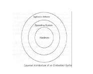
The operating system runs above the hardware, and the application software runs above the Figure 3.1: Embedded Layer Architecture
operating system. The same architecture is applicable to any computer including a desktop computer. However, there are significant differences. It is not compulsory to have an operating system in every embedded system. For small appliances such as remote control units, air conditioners, toys etc., there is no need for an operating system and you can write only the software specific to that application. For applications involving complex processing, it is advisable to have an operating system. In such a case, you need to integrate the application software with the operating system and then transfer the entire software on to the memory chip. Once the software is transferred to the memory chip, the software will continue to run for a long time you don’t need to reload new software.
Now, let us see the details of the various building blocks of the hardware of an embedded system. As shown in Fig. the building blocks are;
- Central Processing Unit (CPU)
- Memory (Read-only Memory and Random Access Memory)
- Input Devices
- Output devices
- Communication interfaces
- Application-specific circuitry
Central Processing Unit (CPU):
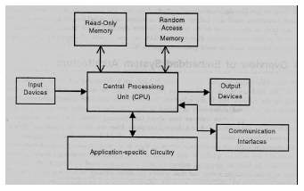
The Central Processing Unit (processor, in short) can be any of the following: microcontroller, microprocessor or Digital Signal Processor (DSP). A micro-controller is a low-cost processor. Its main attraction is that on the chip itself, there will be many other components such as memory,
Figure 3.2: Embedded Architecture
serial communication interface, analog-to digital converter etc. So, for small applications, a micro-controller is the best choice as the number of external components required will be very less. On the other hand, microprocessors are more powerful, but you need to use many external components with them. D5P is used mainly for applications in which signal processing is involved such as audio and video processing.
Memory:
The memory is categorized as Random Access 11emory (RAM) and Read Only Memory (ROM). The contents of the RAM will be erased if power is switched off to the chip, whereas ROM retains the contents even if the power is switched off. So, the firmware is stored in the ROM. When power is switched on, the processor reads the ROM; the program is program is executed.
Input devices:
Unlike the desktops, the input devices to an embedded system have very limited capability. There will be no keyboard or a mouse, and hence interacting with the embedded system is no easy task. Many embedded systems will have a small keypad-you press one key to give a specific command. A keypad may be used to input only the digits. Many embedded systems used in process control do not have any input device for user interaction; they take inputs from sensors or transducers 1’fnd produce electrical signals that are in turn fed to other systems.
Output devices:
The output devices of the embedded systems also have very limited capability. Some embedded systems will have a few Light Emitting Diodes (LEDs) to indicate the health status of the system modules, or for visual indication of alarms. A small Liquid Crystal Display (LCD) may also be used to display some important parameters.
Communication interfaces:
The embedded systems may need to, interact with other embedded systems at they may have to transmit data to a desktop. To facilitate this, the embedded systems are provided with one or a few communication interfaces such as RS232, RS422, RS485, Universal Serial Bus (USB), IEEE 1394, Ethernet etc.
CHAPTER 4
HARDWARE DETAILS OF THE PROJECT
This chapter briefly explains about the Hardware Implementation of the project. It discusses the design and working of the design with the help of block diagram in detail. It explains the features, timer programming, serial communication, interrupts of 8051 microcontroller. It also explains the various modules used in this project.
4.1. PROJECT DESIGN
The execution of the venture configuration can be separated in two sections.
Equipment usage and Firmware usage
Equipment usage bargains in drawing the schematic on the plane paper as indicated by the application, testing the schematic outline over the breadboard utilizing the different IC’s to discover if the outline meets the goal, doing the PCB format of the schematic tried on breadboard, at long last setting up the load up and testing the planned equipment.
The firmware part bargains in programming the microcontroller with the goal that it can control the operation of the IC’s utilized as a part of the usage. In the present work, we have utilized the Orcad outline programming for PCB circuit plan, the Keil µv3 programming advancement device to compose and order the source code, which has been composed in the C dialect. The Proload developer has been utilized to compose this gather code into the microcontroller. The firmware usage is clarified in the following section.
The venture plan and guideline are clarified in this section utilizing the piece outline and circuit graph. The piece outline examines about the required segments of the plan and working condition is clarified utilizing circuit graph and framework wiring chart.
4.1.1 Block Diagram of the Project and its Description
The block diagram of the design is as shown in Fig 3.1. It consists of power supply unit, 8051 microcontroller, MAX232, LCD Display, GSM, TRIAC, Optocouplers, Loads and Feedback circuit . The brief description of each unit is explained as follows.
Block diagram:
µC
KEY PAD


LCD DISPLAY
POWERSUPPLY


RFID READER

GSM MODULE
Figure 4.1: Block Diagram
4.2. POWER SUPPLY
There are many types of power supply. Most are designed to convert high voltage AC mains electricity to a suitable low voltage supply for electronic circuits and other devices. A power supply can be broken down into a series of blocks, each of which performs a particular function.
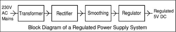
Figure4.2 :Block Diagram of Regulated Power Supply
Each of the blocks is described in more detail below:
- Transformer – steps down high voltage AC mains to low voltage AC.
- Rectifier – converts AC to DC, but the DC output is varying.
- Smoothing – smoothes the DC from varying greatly to a small ripple.
- Regulator – eliminates ripple by setting DC output to a fixed voltage.
Power supplies made from these blocks are described below with a circuit diagram and a graph of their output:
- Transformer only
- Transformer + Rectifier
- Transformer + Rectifier + Smoothing
- Transformer + Rectifier + Smoothing + Regulator
4.2.1. Transformer circuit:
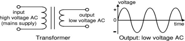
Figure 4.3 Transformer circuit
The low voltage AC output is suitable for lamps, heaters and special AC motors. It is not suitable for electronic circuits unless they include a rectifier and a smoothing capacitor.
4.2.2. Transformer + Rectifier circuit:
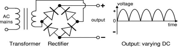
Figure 4.4 Transformer + Rectifier circuit
The varying DC output is suitable for lamps, heaters and standard motors. It is not suitable for electronic circuits unless they include a smoothing capacitor.
4.2.3. Transformer + Rectifier + Smoothing circuit:
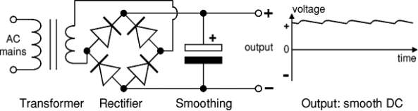
Figure 4.5 Transformer + Rectifier + Smoothing circuit
The smooth DC output has a small ripple. It is suitable for most electronic circuits.
4.2.4. Transformer + Rectifier + Smoothing + Regulator circuit:
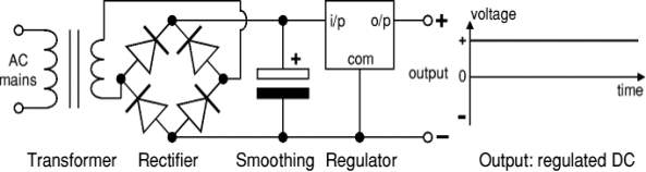
Figure 4.6 Transformer + Rectifier + Smoothing + Regulator circuit
The regulated DC output is very smooth with no ripple. It is suitable for all electronic circuits.

 4.3. MICROCONTROLLER (8051)
33330Ω
The Atmel AT89 arrangement is an Intel 8051-perfect group of 8 bit microcontrollers made by the Atmel Corporation. In light of the Intel 8051 center, the AT89 arrangement stays exceptionally well known as broadly useful microcontrollers, because of their industry standard guideline set, and low unit cost. This permits an awesome measure of legacy code to be reused without adjustment in new applications. While extensively less effective than the fresher AT90 arrangement of AVR microcontrollers, new item improvement has proceeded with the AT89 arrangement for the previously mentioned points of interest. Of later circumstances, the AT89 arrangement has been increased with 8051-cored unique capacity microcontrollers, particularly in the ranges of USB, I²C, SPI and CAN bus controllers, MP3 decoders and hardware PWM.
4.3.1.AT89 Series Microcontrollers
| Device Name | Program Memory | Data Memory |
| AT89C1051 | 1K Flash | 64 Bytes RAM |
| AT89C2051 | 2K Flash | 128 Bytes RAM |
| AT89C51 | 4K Flash | 128 Bytes RAM |
| AT89C52 | 8K Flash | 256 Bytes RAM |
| AT89C55 | 20K Flash | 256 Bytes RAM |
| AT89S51 | 4K Flash | 128 Bytes RAM |
| AT89S52 | 8K Flash | 256 Bytes RAM |
| AT89S53 | 12K Flash | 256 Bytes RAM |
Table 1: list of AT89 microcontrollers
4.3.2 AT89C51 Description
The AT89C51 is a low-control, superior CMOS 8-bit microcomputer with 4K bytes of Flash programmable and erasable read just memory (EPROM). The gadget is fabricated utilizing Atmel’s high-thickness nonvolatile memory innovation and is good with the business standard MCS-51 direction set and stick out. The on-chip Flash permits the program memory to be reconstructed in-framework or by a traditional nonvolatile memory developer. By joining an adaptable 8-bit CPU with Flash on a solid chip, the Atmel AT89C51 is an intense microcomputer which gives an exceptionally adaptable and practical answer for some installed control applications.
4.3.3.Features of AT89C51
- Compatible with MCS-51 Products
- 4K Bytes of In-System Reprogrammable Flash Memory (Endurance: 1,000 Write/Erase Cycles)
- Fully Static Operation: 0 Hz to 24 MHz
- Three-level Program Memory Lock
- 128 x 8-bit Internal RAM
- 32 Programmable I/O Lines
- Two 16-bit Timer/Counters
- Six Interrupt Sources
- Programmable Serial Channel
- Low-power Idle and Power-down Modes
4.3.4.Pin Diagram of AT89C51
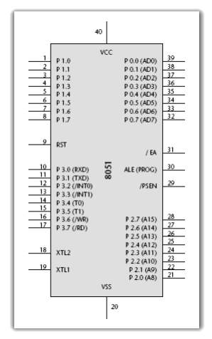
Fig 4.7 Pin diagram of 8051 microcontroller
4.3.5. Basic Pins
PIN 9: This is the reset stick which is utilized reset the microcontroller’s inner registers and ports after beginning up. A high on this stick for two machine cycles while the oscillator is running resets the gadget.
PINS 18 and 19: This microcontroller (8051) has an inherent oscillator speaker subsequently we have to just associate a precious stone at these pins to give clock heartbeats to the circuit.
PINS 40 and 20: The pins 40 and 20 are VCC and GND individually. The 8051 chip needs +5V 500mA to work appropriately, in spite of the fact that there are lower fueled renditions like the Atmel 2051 which is a downsized adaptation of the 8051 which keeps running on +3V.
PINS 29, 30 and 31: This chip contains an inherent blaze memory. So as to program this we have to supply a voltage of +12V at stick 31. On the off chance that outer memory is associated then PIN 31, likewise called EA (outside get to), ought to be associated with ground to show the nearness of outer memory. Stick 30 is called ALE (address hook empower), which is utilized when numerous memory chips are associated with the controller and just a single of them should be chosen. Stick 29 is called PSEN (program store empower). With a specific end goal to utilize the outside memory it is required to give the low voltage (0) on both PSEN and EA pins.
4.3.6.Ports
All the 8051 microcontrollers have 4 I/O ports each involving 8 bits which can be designed as data sources or yields. In like manner, altogether of 32 info/yield pins empowering the microcontroller to be associated with fringe gadgets are accessible for utilize.
Stick arrangement, i.e. regardless of whether it is to be arranged as an info (1) or a yield (0), relies on upon its rationale state. With a specific end goal to design a microcontroller stick as a yield, it is important to apply a rationale zero (0) to fitting I/O port piece. For this situation, voltage level on fitting pin will be 0.
So also, with a specific end goal to arrange a microcontroller stick as an information, it is important to apply a rationale one (1) to fitting port. For this situation, voltage level on fitting pin will be +5V (similar to the case with any TTL input).
PORT P1 (Pins 1 to 8): This port P1 is a universally useful information/yield port which can be utilized for an assortment of interfacing undertakings. Alternate ports P0, P2 and P3 have double parts or extra capacities related with them in light of the setting of their use.
PORT P3 (Pins 10 to 17): The PORT P3 goes about as a typical IO port, yet port P3 has extra capacities, for example, serial transmit and get pins, 2 outside intrude on pins, 2 outer counter sources of info, read and compose pins for memory get to.
PORT P2 (pins 21 to 28): The PORT P2 can likewise be utilized as a universally useful 8 bit port when no outside memory is available, yet in the event that outer memory get to is required then port P2 will go about as an address transport in conjunction with port P0 to get to outside memory. PORT P2 goes about as A8-A15, as can be seen from stick outline.
PORT P0 (pins 32 to 39) PORT P0 can be utilized as a broadly useful 8 bit port when no outside memory is available, however in the event that outer memory get to is required then port P0 goes about as a multiplexed address and information transport that can be utilized to get to outer memory in conjunction with PORT P2. P0 goes about as AD0-AD7, as can be seen from stick outline.
4.3.7. Memory Organization
8051 has two sorts of memory and these are Program Memory and Data Memory. Program Memory (ROM) is utilized to forever spare the program being executed, while Data Memory (RAM) is utilized for incidentally putting away information and transitional outcomes made and utilized amid the operation of the microcontroller. Contingent upon the model being used (we are as yet discussing the 8051 microcontroller family when all is said in done) at most a couple KB of ROM and 128 or 256 bytes of RAM is utilized. Be that as it may, each of the 8051 microcontrollers have a 16-bit tending to transport and are equipped for tending to 64 KB memory.
Program Memory
The main models of the 8051 microcontroller family did not have interior program memory. It was included as an outer separate chip. These models are conspicuous by their mark starting with 803 (for instance 8031 or 8032). Every single later model have a couple KB ROM inserted. Despite the fact that such a measure of memory is adequate for composing the greater part of the projects, there are circumstances when it is important to utilize extra memory too. How does the microcontroller handle outside memory rely on upon the EA stick rationale state.
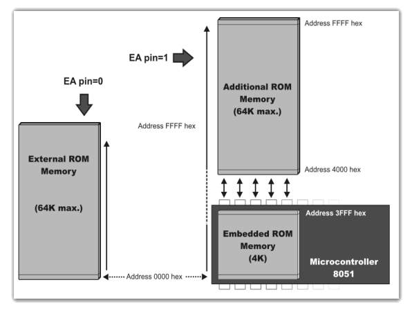
Fig 4.8 Program Memory of 8051
If EA = 0 then the microcontroller totally overlooks inside program memory and executes just the program put away in outside memory. On the off chance that EA = 1 then the microcontroller executes first the program from implicit ROM, then the program put away in outer memory. In both cases, P0 and P2 are not accessible for use since being utilized for information and address transmission. In addition, the ALE and PSEN pins are additionally utilized.
Data Memory
Data Memory is utilized for briefly putting away information and middle outcomes made and utilized amid the operation of the microcontroller. In addition, RAM memory worked in the 8051 family incorporates many registers, for example, equipment counters and clocks, input/yield ports, serial information supports and so on. The past models had 256 RAM areas, while for the later models this number was augmented by extra 128 registers. Be that as it may, the initial 256 memory areas (addresses 0-FFh) are the heart of memory regular to every one of the models having a place with the 8051 family. Areas accessible to the client involve memory space with locations 0-7Fh, i.e. initial 128 registers. This piece of RAM is isolated in a few squares.
The principal piece comprises of 4 banks each including 8 registers signified by R0-R7. Before getting to any of these registers, it is important to choose the bank containing it. The following memory piece (address 20h-2Fh) is bit-addressable, which implies that each piece has its own address (0-7Fh). Since there are 16 such registers, this piece contains altogether of 128 bits with isolated locations (address of bit 0 of the 20h byte is 0, while address of bit 7 of the 2Fh byte is 7Fh). The third gathering of registers possesses addresses 2Fh-7Fh, i.e. 80 areas, and does not have any uncommon capacities or components.
4.3.8. Special Function Registers (SFRs)
Special Function Registers (SFRs) are a kind of control table utilized for running and observing the operation of the microcontroller. Each of these registers and in addition each piece they incorporate, has its name, address in the extent of RAM and unequivocally characterized reason, for example, clock control, intrude on control, serial correspondence control and so forth. Despite the fact that there are 128 memory areas proposed to be possessed by them, the essential center, shared by a wide range of 8051 microcontrollers, has just 21 such registers. Whatever is left of areas are deliberately left abandoned so as to empower the producers to additionally create microcontrollers keeping them good with the past forms. It likewise empowers programs composed quite a while prior for microcontrollers which are out of generation now to be utilized today.
Additional RAM
So as to fulfill the software engineers’ steady crave Data Memory, the makers chose to install an extra memory piece of 128 areas into the most recent forms of the 8051 microcontrollers. Be that as it may, it’s not as basic as it is by all accounts… The issue is that gadgets performing tending to has 1 byte (8 bits) on transfer and is fit for achieving just the initial 256 areas, along these lines. To keep officially existing 8-bit engineering and similarity with other existing models a little trap was finished.
What does it mean? It implies that extra memory piece has similar locations with areas proposed for the SFRs (80h-FFh). Keeping in mind the end goal to separate between these two physically isolated memory spaces, distinctive methods for tending to are utilized. The SFRs memory areas are gotten to by direct tending to, while extra RAM memory areas are gotten to by roundabout tending to.
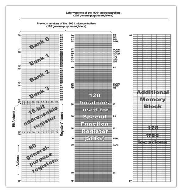
Fig 4.9 Latest Version of 8051
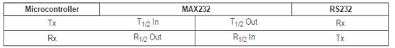
4.4.MAX 232:
Max232 IC is a particular circuit which makes standard voltages as required by RS232 principles. This IC gives best clamor dismissal and extremely solid against releases and shortcircuits.MAX232 IC chips are normally alluded to as line drivers.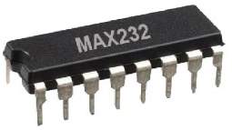
Figure 4.10: MAX232 IC
To guarantee information exchange amongst PC and microcontroller, the baud rate and voltage levels of Microcontroller and PC ought to be the same. The voltage levels of microcontroller are logic1 and rationale 0 i.e., rationale 1 is +5V and rationale 0 is 0V. In any case, for PC, RS232 voltage levels are considered and they are: rationale 1 is taken as – 3V to – 25V and rationale 0 as +3V to +25V. In this way, keeping in mind the end goal to meet these voltage levels, MAX232 IC is utilized. Along these lines this IC changes over RS232 voltage levels to microcontroller voltage levels and the other way around.
4.4.1 Pin Configuration and Functions:
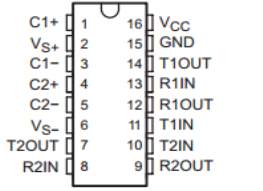
Figure 4.11: MAX 232 Pin diagram
Pin Description:
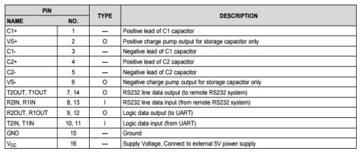
Table 2:MAX232 Pin description
The MAX232 IC is utilized to change over the TTL/CMOS rationale levels to RS232 rationale levels amid serial correspondence of microcontrollers with PC. The controller works at TTL rationale level (0-5V) though the serial correspondence in PC takes a shot at RS232 benchmarks (- 25 V to + 25V). This makes it hard to build up an immediate connection between them to speak with each other.
The halfway connection is given through MAX232. It is a double driver/recipient that incorporates a capacitive voltage generator to supply RS232 voltage levels from a solitary 5V supply. Every collector changes over RS232 contributions to 5V TTL/CMOS levels. These beneficiaries (R1 and R2) can acknowledge ±30V inputs. The drivers (T1 and T2), likewise called transmitters, change over the TTL/CMOS input level into RS232 level.
The transmitters take contribution from controller’s serial transmission stick and send the yield to RS232’s collector. The beneficiaries, then again, take contribution from transmission stick of RS232 serial port and give serial yield to microcontroller’s recipient stick. MAX232 needs four outside capacitors whose esteem ranges from 1µF to 22µF.
Features:
Operates From a Single 5-V Power Supply With 1.0-µF Charge-Pump Capacitors
Operates up to 120 kbit/s
Two Drivers and Two Receivers
±30-V Input Levels
Low Supply Current: 8 mA Typical
Applications:
- TIA/EIA-232-F
- Battery-Powered Systems
- Terminals
- Modems
- Computers
4.5. LIQUID CRYSTAL DISPLAY:
LCD remains for Liquid Crystal Display. LCD is finding across the board utilize supplanting LEDs (seven portion LEDs or other multi section LEDs) as a result of the accompanying reasons:
1. The declining costs of LCDs.
2. The capacity to show numbers, characters and representation. This is as opposed to LEDs, which are restricted to numbers and a couple characters.
3. Joining of a reviving controller into the LCD, in this manner easing the CPU of the errand of invigorating the LCD. Interestingly, the LED must be invigorated by the CPU to continue showing the information.
4. Simplicity of programming for characters and design.
.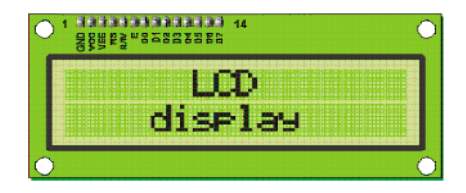
Fig 4.12:LCD display
A model depicted here is at its minimal effort and awesome conceivable outcomes most much of the time utilized as a part of practice. It depends on the HD44780 microcontroller (Hitachi) and can show messages in two lines with 16 characters each. It shows every one of the letters in order, Greek letters, accentuation marks, scientific images and so on. What’s more, it is conceivable to show images that client makes up all alone.
Programmed moving message in plain view (move left and right), appearance of the pointer, backdrop illumination and so on are considered as helpful attributes.
4.5.1. Pins Functions:
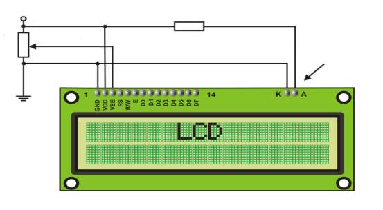
There are sticks along one side of the little printed board utilized for association with the microcontroller. There are aggregate of 14 pins set apart with numbers (16 on the off chance that the foundation light is inherent). Their capacity is portrayed in the table 3.6
4.5.2. LCD screen:
LCD screen shown in figure 3.15 comprises of two lines with 16 characters each. Each character comprises of 5×7 speck lattice. Differentiate in plain view relies on upon the power supply voltage and whether messages are shown in maybe a couple lines. Therefore, factor voltage 0-Vdd is connected on stick set apart as Vee. Trimmer potentiometer is normally utilized for that reason. A few forms of presentations have worked in backdrop illumination (blue or green diodes). At the point when utilized amid working, a resistor for current impediment ought to be utilized (like with any LE diode).
Contrast
LCD backlight
330R
5k
Figure 4.13: LCD connection
4.5.3. LCD Basic Commands:
All information exchanged to LCD through yields D0-D7 will be translated as orders or as information, which relies on upon rationale state on stick RS: RS = 1 – Bits D0 – D7 are locations of characters that ought to be shown. Worked in processor addresses worked in “guide of characters” and shows comparing images. Showing position is dictated by DDRAM address. This address is either beforehand characterized or the address of already exchanged character is consequently increased.
RS = 0 – Bits D0 – D7 are charges which decide show mode. Rundown of orders which LCD perceives are extremely important to write the code for LCD. The below table 3.4 shows the LCD commands which are useful in the writing of code to display the data.
Table 4: LCD commands table
| Command | RS | RW | D7 | D6 | D5 | D4 | D3 | D2 | D1 | D0 | Execution
Time |
|
| Clear display | 0 | 0 | 0 | 0 | 0 | 0 | 0 | 0 | 0 | 1 | 1.64Ms | |
| Cursor home | 0 | 0 | 0 | 0 | 0 | 0 | 0 | 0 | 1 | x | 1.64mS | |
| Entry mode set | 0 | 0 | 0 | 0 | 0 | 0 | 0 | 1 | I/D | S | 40uS | |
| Display on/off control | 0 | 0 | 0 | 0 | 0 | 0 | 1 | D | U | B | 40uS | |
| Cursor/Display Shift | 0 | 0 | 0 | 0 | 0 | 1 | D/C | R/L | X | x | 40uS | |
| Function set | 0 | 0 | 0 | 0 | 1 | DL | N | F | X | x | 40uS | |
| Set CGRAM address | 0 | 0 | 0 | 1 | CGRAM address | 40uS | ||||||
| Set DDRAM address | 0 | 0 | 1 | DDRAM address | 40uS | |||||||
| Read “BUSY” flag (BF) | 0 | 1 | BF | DDRAM address | – | |||||||
| Write to CGRAM or DDRAM | 1 | 0 | D7 | D6 | D5 | D4 | D3 | D2 | D1 | D0 | 40uS | |
| Read from CGRAM or DDRAM | 1 | 1 | D7 | D6 | D5 | D4 | D3 | D2 | D1 | D0 | 40uS | |
Table 4: LCD commands table
I/D 1 = Increment (by 1) R/L 1 = Shift right
0 = Decrement (by 1) 0 = Shift left
S 1 = Display shift on DL 1 = 8-bit interface
0 = Display shift off 0 = 4-bit interface
D 1 = Display on N 1 = Display in two lines
0 = Display off 0 = Display in one line
U 1 = Cursor on F 1 = Character format 5×10 dots
0 = Cursor off 0 = Character format 5×7 dots
B 1 = Cursor blink on D/C 1 = Display shift
0 = Cursor blink off 0 = Cursor shift
4.5.4. LCD Connection:
Contingent upon what number of lines are utilized for association with the microcontroller, there are 8-bit and 4-bit LCD modes. The fitting mode is resolved toward the start of the procedure in a stage called “instatement”. In the principal case, the information are exchanged through yields D0-D7 as it has been as of now clarified. If there should be an occurrence of 4-bit LED mode, for sparing important I/O pins of the microcontroller, there are just 4 higher bits (D4-D7) utilized for correspondence, while other might be left detached.
Subsequently, every information is sent to LCD in two stages: four higher bits are sent first (that ordinarily would be sent through lines D4-D7), four lower bits are sent a short time later. With the assistance of introduction, LCD will effectively associate and decipher every information got. Furthermore, as to the way that information are once in a while perused from LCD (information principally are exchanged from microcontroller to LCD) one more I/O stick might be spared by straightforward associating R/W stick to the Ground. Such sparing has its cost. Despite the fact that message showing will be typically performed, it won’t be conceivable to peruse from occupied banner since it is unrealistic to peruse from show.
4.5.5. LCD Initialization:
Once the power supply is turned on, LCD is consequently cleared. This procedure goes on for roughly 15mS. From that point onward, show is prepared to work. The method of working is set naturally. This implies:
1. Display is cleared
2. Mode
DL = 1 Communication through 8-bit interface
N = 0 Messages are displayed in one line
F = 0 Character font 5 x 8 dots
3. Display/Cursor on/off
D = 0 Display off
U = 0 Cursor off
B = 0 Cursor blink off
3. Character entry
ID = 1 Addresses on display are automatically incremented by 1
S = 0 Display shift off
4.6 GSM MODEM:
The short message framework (SMS) of a standard cell phone can be utilized for considerably more than simply trading enigmatic message. This application finds a modest portable working for controlling outer types of gear. The SMS benefit gives by the specialist organizations are similarly minimal effort. Henceforth the framework is exceedingly proficient and minimal effort.
Cell phones have turned into a boundless methods for correspondence. It turns into a piece of regular daily existence with always individuals getting a charge out of the administration and additional flexibility they give. It takes a shot at the premise of Global System for Mobile Communication (GSM). A supporter from any frameworks can get to media transmission benefits by utilizing a Subscriber Identity Module (SIM) card in a handset appropriate for the system on the went to framework The Short Message Service permits instant messages to be sent and got to and from cell phones. The content can contain words or numbers or an alphanumeric blend. Since Simple individual – to – individual informing is such an imperative segment of aggregate SMS activity volumes, anything that improves message era and additionally broadened utility of the SMS being sent is an essential empowering influence of Short Message Service.
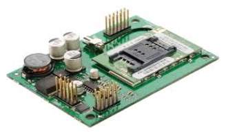
Figure 4.17:GSM Module
The main aim of this project is to control the car engine. We will connect Hardware kit to car engine. The hardware kit consists of microcontroller and GSM modem
A GSM modem is a particular sort of modem which acknowledges a SIM card, and works over a membership to a versatile administrator, much the same as a cell phone. From the versatile administrator viewpoint, a GSM modem looks simply like a cell phone.
At the point when a GSM modem is associated with a PC, this permits the PC to utilize the GSM modem to impart over the portable system. While these GSM modems are most as often as possible used to give versatile web availability, a hefty portion of them can likewise be utilized for sending and getting SMS and MMS messages.
Presently SMS Light can send and get SMS and MMS Messages utilizing a GSM modem:
A GSM modem can be a committed modem gadget with a serial, USB or Bluetooth association, or it can be a cell phone that gives GSM modem capacities.
With the end goal of this archive, the term GSM modem is utilized as a non specific term to allude to any modem that backings at least one of the conventions in the GSM transformative family, including the 2.5G innovations GPRS and EDGE, and additionally the 3G advances WCDMA, UMTS, HSDPA and HSUPA.
A GSM modem uncovered an interface that permits applications, for example, Now SMS to send and get messages over the modem interface. The versatile administrator charges for this message sending and getting as though it was performed specifically on a cell phone. To play out these errands, a GSM modem must support a “stretched out AT summon set” for sending/getting SMS messages, as characterized in the http://www.etsi.orgETSI GSM 07.05 and http://www.3gpp.org/ftp/specs/html-data/27005.htm3GPP TS 27.005 particulars.
GSM modems can be a snappy and productive approach to begin with SMS, on the grounds that an extraordinary membership to a SMS specialist organization is not required. In many parts of the world, GSM modems are a practical answer for accepting SMS messages, on the grounds that the sender is paying for the message conveyance.
A GSM modem can be a devoted modem gadget with a serial, USB or Bluetooth association, for example, the Falcon Samba 75. (Different producers of committed GSM modem gadgets incorporate Wavecom, Multitech and iTegno. We’ve likewise audited various modems on our http://www.nowsms.com/tag/gsm-modemtechnical bolster blog.) To start, embed a GSM SIM card into the modem and associate it to an accessible USB port on your PC.
A GSM modem could likewise be a standard GSM cell phone with the suitable link and programming driver to interface with a serial port or USB port on your PC. Any telephone that backings the “reached out AT charge set” for sending/getting SMS messages, as characterized in http://www.etsi.orgETSI GSM 07.05 as well as http://www.3gpp.org/ftp/specs/html-information/27005.htm3GPP TS 27.005, can be bolstered by the Now SMS and MMS Gateway. Take note of that not every single cell phone bolster this modem interface.
Because of some similarity issues that can exist with cell phones, utilizing a devoted GSM modem is typically desirable over a GSM cell phone. This is a greater amount of an issue with MMS informing, where on the off chance that you wish to have the capacity to get inbound MMS messages with the passage, the modem interface on most GSM telephones will just permit you to send MMS messages. This is on the grounds that the cell phone consequently forms got MMS message warnings without sending them by means of the modem interface. It ought to likewise be noticed that not all telephones bolster the modem interface for sending and getting SMS messages. Specifically, most advanced cells, including Blackberries, iPhone, and Windows Mobile gadgets, don’t bolster this GSM modem interface for sending and getting SMS messages at all by any stretch of the imagination. Also, Nokia telephones that utilization the S60 (Series 60) interface, which is Symbian based, just bolster sending SMS messages by means of the modem interface, and don’t bolster accepting SMS by means of the modem interface.
4.6.1.The Future of GSM:
GSM together with other technologies is part of an evolution of wireless mobile telecommunication that includes High-Speed Circuit-Switched Data (HSCSD), General Packet Radio System (GPRS), Enhanced Data rate for GSM Evolution (EDGE), and Universal Mobile Telecommunications Service (UMTS).
4.6.2.GSM Network Operators:
T-Mobile and Cingular operate GSM networks in the United States on the 1,900 MHz band. GSM networks in other countries operate at 900, 1,800, or 1,900 MHz.
GSM (Global System for Mobile Communications):
Originally from Group Special Mobile) is the most popular standard for mobile telephony systems in the world. The GSM Association, its promoting industry trade organization of mobile phone carriers and manufacturers, estimates that 80% of the global mobile market uses the standard.[1] GSM is used by over 1.5 billionpeople[2] across more than 212 countries and territories.[3] This ubiquity means that subscribers can use their phones throughout the world, enabled by international roaming arrangements between mobile network operators. GSM differs from its predecessor technologies in that both signaling and speech channels are digital, and thus GSM is considered a second generation (2G) mobile phone system. This also facilitates the wide-spread implementation of data communication applications into the system.
The GSM standard has been an advantage to both consumers, who may benefit from the ability to roam and switch carriers without replacing phones, and also to network operators, who can choose equipment from many GSM equipment vendors.[4] GSM also pioneered low-cost implementation of the short message service (SMS), also called text messaging, which has since been supported on other mobile phone standards as well. The standard includes a worldwide emergency telephone number feature (112).[5]
Newer versions of the standard were backward-compatible with the original GSM system. For example, Release ’97 of the standard added packet data capabilities by means of General Packet Radio Service (GPRS). Release ’99 introduced higher speed data transmission using Enhanced Data Rates for GSM Evolution (EDGE).
4.6.3.GSM carrier frequencies:
GSM networks operate in a number of different carrier frequency ranges (separated into GSM frequency ranges for 2G and UMTS frequency bands for 3G), with most 2GGSM networks operating in the 900 MHz or 1800 MHz bands. Where these bands were already allocated, the 850 MHz and 1900 MHz bands were used instead (for example in Canada and the United States). In rare cases the 400 and 450 MHz frequency bands are assigned in some countries because they were previously used for first-generation systems.
Most 3G networks in Europe operate in the 2100 MHz frequency band.
Regardless of the frequency selected by an operator, it is divided into timeslots for individual phones to use. This allows eight full-rate or sixteen half-rate speech channels per radio frequency. These eight radio timeslots (or eight burst periods) are grouped into a TDMA frame. Half rate channels use alternate frames in the same timeslot. The channel data rate for all 8 channels is 270.833 Kbit/s, and the frame duration is 4.615 ms.
The transmission power in the handset is limited to a maximum of 2 watts in GSM850/900 and 1 watt in GSM1800/1900.
Check if your GSM phone or modem supports SMS text mode:
To check if your modem supports this text mode, you can try the following command:
AT+CMGF=1 <ENTER>
If the modem responds with “OK” this mode is supported. Please note that using this mode it is only possible to send simple text messages. It is not possible to send multipart, Unicode, data and other types of messages.
Setting up the modem
If the modem contains a SIM card with is secured with a PIN code, we have to enter this pin code first:
AT+CPIN=”0000″ <ENTER> (replace 0000 with your PIN code):
Please not that in most cases you have only 3 attempts to set the correct PIN code. After setting the PIN code, wait some seconds before issuing the next command to give the modem some time to register with the GSM network.
In order to send a SMS, the modem has to be put in SMS text mode first using the following command:
AT+CMGF=1 <ENTER>
In text mode there are some additional parameters that can be set. Using the following command we can read the current values:
AT+CSMP? <ENTER>
The modem wills response with a string like this:
+CSMP: 1, 169, 0,0OK
The first value is a combination of some option bits:
| bit 7 | RP | Reply path, not used in text mode |
| bit 6 | UDHI | User Data Header Information |
| bit 5 | SRR | Set this bit to request a delivery report |
| bit 3,4 | VPF | Validity Period, set b4=1 if a VP value is present |
| bit 2 | RD | Reject Duplicates, do not return a message ID when a message with the same destination and ID is still pending |
| bit 0,1 | MTI | Message Type Indicatorb1=0 & b0=0 -> SMS-DELIVERb1=0 & b0=1 -> SMS-SUBMIT |
Bit 0 of the message is always set when sending messages (SMS-SUBMIT). So the first value should be 1 or higher. The second parameter sets the Validity Period of the message. This value is encoded as follows:
| 0 – 143 | (VP + 1) x 5 minutes |
| 144 – 167 | 12 Hours + ((VP-143) x 30 minutes) |
| 168 – 196 | (VP-166) x 1 day |
| 197 – 255 | (VP-192) x 1 week |
The third parameter contains the PID (Protocol Identifier). This parameter is only used for advanced messaging. The fourth parameter contains the DCS (Data Coding Scheme). This parameter is used to select the character set/message type. When setting the DCS parameter to ‘0’ standard 7 bit text is send. When setting this parameter to ’16’ the message is sent as a flash message.
To send a message with a validity period of 1 day, the parameters have to be set like this:
Bit 0 and 4 of the first field has to be set, so the first value will become 1 + 16 = 17.
Send the following command to the modem to set this parameters:
AT+CSMP=17, 167,0,16 <ENTER>
If the modem responds with “OK” ,the modem is ready to send (flash) text messages with a validity period of 1 day.
Sending the message
To send the SMS message, type the following command:
AT+CMGS=”+31638740161″ <ENTER>
Replace the above phone number with your own cell phone number. The modem will respond with:
>
You can now type the message text and send the message using the <CTRL>-<Z> key combination:
Hello World! <CTRL-Z>
After some seconds the modem will respond with the message ID of the message, indicating that the message was sent correctly:
+CMGS: 62
The message will arrive on the mobile phone shortly.
Sending an Unicode SMS message
Some modems also have the capability to send Unicode or UCS2 messages without encoding a PDU. You can send Unicode messages by only converting the Unicode data to a HEX string and send this string to the modem.
To check whether your modem supports this mode, just type the following command:
AT+CSCS=?
This command displays the codepages supported by the modem. The modem will respond like this:
+CSCS: (“GSM”,”PCCP437″,”CUSTOM”,”HEX”)
If this string contains “HEX” or “UCS2”, Unicode seems to be supported. To specify that you will use an HEX string to send the message, set the codepage to “HEX” or “UCS2” depending on the modem response. In our example we will set the modem to “HEX”:
AT+CSCS=”HEX” <ENTER>
Next, we have to specify the correct DCS (Data Coding Scheme) for Unicode messages, which is 0x08. We can set this value by changing the fourth parameter of the AT+CSMP command to ‘8’:
AT+CSMP=1,167,0,8<ENTER>
The modem is now ready to send messages as Unicode. Now is the time to send the actual message:
AT+CMGS=”+31638740161″ <ENTER>
Replace the above phone number with your own cell phone number. The modem will respond with:
>
The only thing you have to program by yourself, is a simple routine which converts the Unicode string to an hexadecimal string like this:
مرحبا
Which is ‘Hello’ in Arabic will be converted like this:
“06450631062D06280627”
You can send this hexadecimal string to the modem:
06450631062D06280627 <CTRL-Z>
After some seconds the modem will respond with the message ID of the message, indicating that the message was sent correctly:
+CMGS: 63
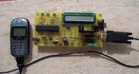
Figure 4.18:GSM module connection to phone
The message will arrive on the mobile phone shortly.
4.7.TRIAC
Triac is an individual from the thyristor family that be utilized as a strong state control exchanging gadget yet more vitally it is a “bidirectional” gadget. At the end of the day, a Triac can be activated into conduction by both positive and negative voltages connected to its Anode and with both positive and negative trigger heartbeats connected to its Gate terminal making it a two-quadrant exchanging Gate controlled gadget.
A Triac acts simply like two ordinary thyristors associated together in opposite parallel (consecutive) as for each other and in view of this game plan the two thyristors share a typical Gate terminal all inside a solitary three-terminal bundle.
Since a triac leads in both headings of a sinusoidal waveform, the idea of an Anode terminal and a Cathode terminal used to distinguish the principle control terminals of a thyristor are supplanted with recognizable pieces of proof of: MT1, for Main Terminal 1 and MT2 for Main Terminal 2 with the Gate terminal G referenced the same.
In most AC exchanging applications, the triac entryway terminal is related with the MT1terminal, like the door cathode relationship of the thyristor or the base-producer relationship of the transistor. The development, P-N doping and schematic image used to represent a Triac is given beneath.
4.7.1.Triac Symbol and Construction
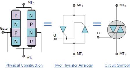
Fig 4.19 TRIAC symbol and construction
We now know that a “triac” is a 4-layer, PNPN in the positive direction and a NPNP in the negative direction, three-terminal bidirectional device that blocks current in its “OFF” state acting like an open-circuit switch, but unlike a conventional thyristor, the triac can conduct current in either direction when triggered by a single gate pulse. Then a triac has four possible triggering modes of operation as follows.
- Ι + Mode = MT2 current positive (+ve), Gate current positive (+ve)
- Ι – Mode = MT2 current positive (+ve), Gate current negative (-ve)
- ΙΙΙ + Mode = MT2 current negative (-ve), Gate current positive (+ve)
- ΙΙΙ – Mode = MT2 current negative (-ve), Gate current negative (-ve)
And these four modes in which a triac can be operated are shown using the triacs I-V characteristics curves.
4.7.2.Triac I-V Characteristics Curves
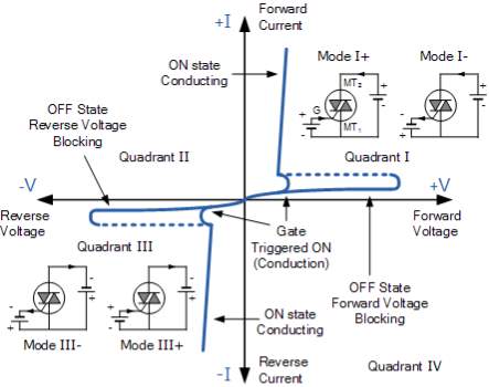
Fig 4.20 TRIAC I-V characteristic curve
In Quadrant Ι, the triac is normally activated into conduction by a positive entryway present, marked above as mode Ι+. Be that as it may, it can likewise be activated by a negative entryway current, mode Ι–. Correspondingly, in Quadrant Ιιι, activating with a negative door current, –ΙG is likewise normal, mode Ιιι– alongside mode Ιιι+. Modes Ι– and Ιιι+ are, in any case, less delicate setups requiring a more prominent entryway current to bring about activating than the more typical triac activating methods of Ι+ and Ιιι–.
Additionally, much the same as silicon controlled rectifiers (SCR’s), triac’s likewise require a base holding current IH to keep up conduction at the waveforms traverse point. At that point despite the fact that the two thyristors are consolidated into one single triac gadget, regardless they show individual electrical attributes, for example, unique breakdown voltages, holding streams and trigger voltage levels precisely the same as we would anticipate from a solitary SCR gadget.
The Triac is most usually utilized semiconductor gadget for exchanging and power control of AC frameworks as the triac can be exchanged “ON” by either a positive or negative Gate beat, paying little respect to the extremity of the AC supply around then. This makes the triac perfect to control a light or AC engine stack with an exceptionally essential triac exchanging circuit given beneath.
4.7.3.Triac Switching Circuit
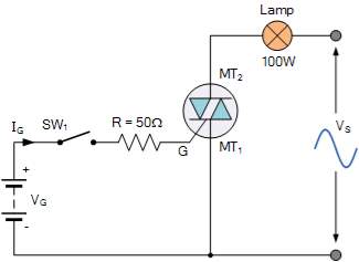
Fig 4.21 TRIAC switching circuit
The circuit above demonstrates a straightforward DC activated triac control exchanging circuit. With switch SW1 open, no present streams into the Gate of the triac and the light is subsequently “OFF”. At the point when SW1 is shut, Gate current is connected to the triac from the battery supply VG through resistor R and the triac is crashed into full conduction acting like a shut switch and full power is drawn by the light from the sinusoidal supply.
As the battery supplies a positive Gate current to the triac at whatever point switch SW1 is shut, the triac is in this manner constantly gated in modes Ι+ and Ιιι+ paying little mind to the extremity of terminal MT2.
Obviously, the issue with this straightforward triac exchanging circuit is that we would require an extra positive or negative Gate supply to trigger the triac into conduction. Be that as it may, we can likewise trigger the triac utilizing the genuine AC supply voltage itself as the dooractivating voltage. Consider the circuit beneath.
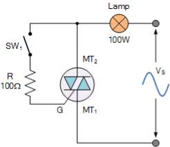
Fig 4.22 TRIAC switching circuit 2
The circuit demonstrates a triac utilized as a basic static AC control switch giving an “ON”- “OFF” capacity comparative in operation to the past DC circuit. At the point when switch SW1 is open, the triac goes about as an open switch and the light passes zero current. At the point when SW1 is shut the triac is gated “ON” by means of current restricting resistor R and self-hooks soon after the begin of every half-cycle, accordingly changing full energy to the light load.
As the supply is sinusoidal AC, the triac naturally unlatches toward the finish of every AC half-cycle as the prompt supply voltage and in this way the heap current quickly tumbles to zero yet re-hooks again utilizing the inverse thyristor half on the following half cycle the length of the switch stays shut. This sort of exchanging control is for the most part called full-wave control because of the way that both parts of the sine wave are being controlled.
As the triac is viably two consecutive associated SCR’s, we can take this triac exchanging circuit assist by changing how the entryway is activated as demonstrated as follows.4.7.4. Modified Triac Switching Circuit
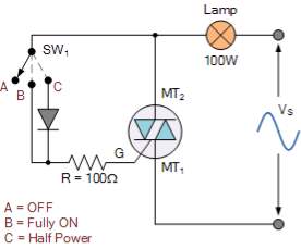
Fig 4.23 Modified TRIAC switching circuit
As above, if switch SW1 is open at position A, there is no gate current and the lamp is “OFF”. If the switch is moved to position B gate current flows at every half cycle the same as before and full power is drawn by the lamp as the triac operates in modes Ι+and ΙΙΙ–.
However this time when the switch is connected to position C, the diode will prevent the triggering of the gate when MT2 is negative as the diode is reverse biased. Thus the triac only conducts on the positive half-cycles operating in mode I+ only and the lamp will light at half power. Then depending upon the position of the switch the load is Off, at Half Power or Fully ON.
4.7.5.Triac Phase Control
Another common type of triac switching circuit uses phase control to vary the amount of voltage, and therefore power applied to a load, in this case a motor, for both the positive and negative halves of the input waveform. This type of AC motor speed control gives a fully variable and linear control because the voltage can be adjusted from zero to the full applied voltage as shown.
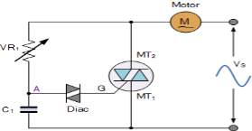
Fig 4.24 TRIAC phase control
This essential stage activating circuit utilizes the triac in arrangement with the engine over an AC sinusoidal supply. The variable resistor, VR1 is utilized to control the measure of stage move on the door of the triac which thus controls the measure of voltage connected to the engine by turning it ON at various circumstances amid the AC cycle.
The triac’s activating voltage is gotten from the VR1 – C1 mix through the Diac (The diac is a bidirectional semiconductor gadget that gives a sharp trigger current heartbeat to completely turn-ON the triac).
Toward the begin of each cycle, C1 energizes by means of the variable resistor, VR1. This proceeds until the voltage crosswise over C1 is adequate to trigger the diac into conduction which thus permits capacitor, C1 to release into the door of the triac turning it “ON”.
Once the triac is activated into conduction and immerses, it adequately shorts out the entryway activating stage control circuit associated in parallel crosswise over it and the triac takes control for the rest of the half-cycle.
As we have seen over, the triac kills consequently toward the finish of the half-cycle and the VR1 – C1 activating procedure begins again on the following half cycle.
Nonetheless, in light of the fact that the triac requires contrasting measures of door current in each exchanging method of operation, for instance Ι+ and Ιιι–, a triac is in this way deviated implying that it may not trigger at precisely the same for every positive and negative half cycle.
This straightforward triac speed control circuit is appropriate for AC engine speed control as well as for light dimmers and electrical radiator control and in actuality is fundamentally the same as a triac light dimmer utilized as a part of many homes. Be that as it may, a business triac dimmer ought not be utilized as an engine speed controller as by and large triac light dimmers are expected to be utilized with resistive loads just, for example, brilliant lights.
At that point we can end this Triac Tutorial by compressing its principle focuses as takes after:
A “Triac” is another 4-layer, 3-terminal thyristor gadget like the SCR.
The Triac can be activated into conduction in either heading.
There are four conceivable activating modes for a Triac, of which 2 are favored.
Electrical AC control utilizing a Triac is to a great degree compelling when utilized appropriately to control resistive sort loads, for example, brilliant lights, radiators or little all inclusive engines usually found in compact power instruments and little apparatuses.
4.8.OPTOCOUPLERS
There are numerous circumstances where signs and information should be exchanged starting with one subsystem then onto the next inside a bit of hardware gear, or starting with one bit of hardware then onto the next, without making a direct ohmic electrical association. Regularly this is on account of the source and goal are (or might be now and again) at altogether different voltage levels, similar to a microchip which is working from 5V DC however being utilized to control a triac which is exchanging 240V AC. In such circumstances the connection between the two must be a disengaged one, to shield the chip from overvoltage harm.
Transfers can obviously give this sort of disconnection, however even little transfers have a tendency to be genuinely cumbersome contrasted and ICs and large portions of today’s other small scale circuit segments. Since they are electro-mechanical, transfers are likewise not as solid .and just prepared to do generally low speed operation. Where little size, higher speed and more prominent unwavering quality are critical, a vastly improved option is to utilize an optocoupler.
Optocouplers utilize a light emission to transmit the signs or information over an electrical obstruction, and accomplish great confinement. Optocouplers regularly arrive in a little 6-stick or 8-stick IC bundle, however are basically a blend of two unmistakable gadgets: an optical transmitter, commonly a gallium arsenide LED (light-producing diode) and an optical beneficiary, for example, a phototransistor or light-activated diac. The two are isolated by a straightforward hindrance which obstructs any electrical current stream between the two, however allows the section of light.
An optocoupler is a mix of a light source and a photosensitive locator. In the optocoupler, or photon coupled match, the coupling is accomplished by light being created on one side of a straightforward protecting crevice and being identified on the opposite side of the hole without an electrical association between the two sides (aside from a minor measure of coupling capacitance). In the Fairchild Semiconductor optocouplers, the light is created by an infrared light transmitting diode, and the photograph locator is a silicon diode which drives an intensifier, e.g., transistor. The affectability of the silicon material tops at the wavelength transmitted by the LED, giving greatest flag coupling.
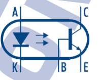
Fig 4.25 Circuit symbol of Optocoupler
Generally the electrical associations with the LED area are conveyed out to the pins on one side of the bundle and those for the phototransistor or diac to the opposite side, to physically isolate them however much as could reasonably be expected. This as a rule permits optocouplers to withstand voltages of anyplace in the vicinity of 500V and 7500V amongst information and yield. Optocouplers are basically computerized or exchanging gadgets, so they are best to transfer either on-off control signals or advanced information. Simple signs can be exchanged by methods for recurrence or heartbeat width balance.
4.8.1. Key Parameters:
The most essential parameter for most optocouplers is their exchange proficiency, generally measured as far as their present exchange proportion or CTR. This is essentially the proportion between a present change in the yield transistor and the present change in the info LED which created it. Run of the mill values for CTR go from 10% to half for gadgets with a yield phototransistor and up to 2000% or so for those with a Darlington transistor combine in the yield.
Other optocoupler parameters incorporate the yield transistor’s greatest authority producer voltage rating VCE(max), which constrains the supply voltage in the yield circuit; the info LEDs most extreme current rating IF(max), which is utilized to ascertain the base an incentive for its arrangement resistor; and the optocoupler’s data transmission, which decides the most noteworthy flag recurrence that can be exchanged through it . decided predominantly by interior gadget development and the execution of the yield phototransistor. Run of the mill optocouplers with a solitary yield phototransistor may have a transmission capacity of 200 – 300kHz, while those with a Darlington combine are more often than not around 10 times lower, at around 20 – 30kHz.
How They are Used:
Fundamentally the most straightforward approach to imagine an optocoupler is as far as its two principle parts: the information LED and the yield transistor or diac. As the two are electrically detached, this gives a considerable lot of adaptability with regards to associating them into circuit. All we truly need to do is work out an advantageous method for turning the info LED on and off, and utilizing the subsequent exchanging of the phototransistor/diac to produce a yield waveform or rationale flag that is perfect with our yield hardware.
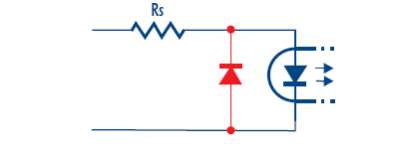
Fig.4.26: Protecting the LED against reverse voltage.
The optocoupler used in this project is MCT2E and eight such optocouplers are used here.The features, description and applications of this IC is discussed in the next topics.
Description:
The MCT2E series of optically coupled isolators consist of infrared light emitting diode and NPN silicon photo transistor in a standard 6 pin dual in line plastic package.
4.8.2 Features:
- Options :-
10mm lead spread – add G after part no.
Surface mount – add SM after part no.
Tape and reel – add SMT&R after part no.
- High Isolation Voltage (5.3kVRMS ,7.5kVPK ).
- All electrical parameters 100% tested.
- Custom electrical selections available.
4.8.3.ABSOLUTE MAXIMUM RATINGS
(25°C unless otherwise specified)
Storage Temperature -55°C to + 150°C
Operating Temperature -55°C to + 100°C
Lead Soldering Temperature
(1/16 inch (1.6mm) from case for 10 secs) 260°C
Input diode
Forward Current 60mA
Reverse Voltage 6V
Power Dissipation 105mW
Output transistor
Collector-emitter Voltage BVCEO 30V
Collector-base Voltage BVCBO 70V
Emitter-collector Voltage BVECO 6V
Power Dissipation 160mW
Power dissipation
Total Power Dissipation 200mW
(linearly 2.67mW/°C above 25°C)
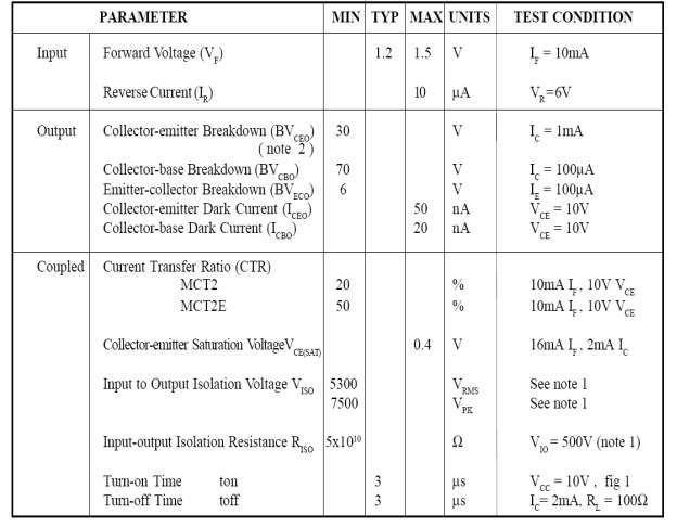
Table 5:Electrical Characteristics
4.8.4 APPLICATIONS
DC engine controllers
Mechanical frameworks controllers
Measuring instruments
Flag transmission between frameworks of various possibilities and impedances
4.9.SERIAL COMMUNICATION IN 8051
One of the 8051’s numerous effective elements is its coordinated UART, also called a serial port. The way that the 8051 has an incorporated serial port implies that you may effectively read and compose qualities to the serial port. On the off chance that it were not for the coordinated serial port, written work a byte to a serial line would be a fairly monotonous process requiring turning on and off one of the I/O lines in quick progression to appropriately “check out” every individual piece, including begin bits, stop bits, and equality bits.
Nonetheless, we don’t need. Rather, we just need to design the serial port’s operation mode and baud rate. Once designed, we should simply write to a SFR to compose an incentive to the serial port or read the same SFR to peruse an incentive from the serial port. The 8051 will consequently tell us when it has wrapped up the character we composed and will likewise tell us at whatever point it has gotten a byte with the goal that we can prepare it. We don’t need to stress over transmission at the bit level – which spares us a considerable amount of coding and handling time.
4.9.1. Setting the Serial Port Mode
The primary thing we should do when utilizing the 8051’s incorporated serial port is, clearly, arrange it. This gives us a chance to tell the 8051 what number of information bits we need, the baud rate we will utilize, and how the baud rate will be resolved. To begin with, we should display the “Serial Control” (SCON) SFR and characterize what each piece of the SFR speaks to
| Bit | Name | Explanation |
| 7 | SM0 | Serial Port Mode Bit 0 |
| 6 | SM1 | Serial Port Mode Bit 1 |
| 5 | SM2 | Multiprocessor Communications Enable |
| 4 | REN | Receiver Enable (This bit must be set in order to receive characters) |
| 3 | TB8 | Transmit Bit 8 (The 9th bit to transmit in mode 2 and 3) |
| 2 | RB8 | Receive Bit 8 (The 9th bit received in mode 2 and 3) |
| 1 | TI | Transmit Flag (Set when a byte has been completely transmitted) |
| 0 | RI | Receive Flag (Set when a byte has been completely received) |
Table 6:Pins and Description of serial port modes
Additionally, it is necessary to define the function of SM0 and SM1 by an additional table:
| SM0 | SM1 | Serial Mode | Explanation | Baud Rate |
| 0 | 0 | 0 | 8-bit Shift Register | Oscillator / 12 |
| 0 | 1 | 1 | 8-bit UART | Set by Timer 1 (*) |
| 1 | 0 | 2 | 9-bit UART | Oscillator / 32 (*) |
| 1 | 1 | 3 | 9-bit UART | Set by Timer 1 (*) |
Table 7: Baud Rate calculation for serial port modes
NOTE: The baud rate indicated in this table is doubled if PCON.7 is set.
The SCON SFR permits us to design the Serial Port. Hence, we’ll experience each piece and audit its capacity. The initial four (bits 4 through 7) are design bits.
Bits SM0 and SM1 let us set the serial mode to an incentive in the vicinity of 0 and 3, comprehensive. The four modes are characterized in the diagram promptly above. As should be obvious, choosing the Serial Mode chooses the method of operation (8-bit/9-bit, UART or Shift Register) and furthermore decides how the baud rate will be ascertained. In modes 0 and 2 the baud rate is settled in light of the oscillator’s recurrence. In modes 1 and 3 the baud rate is variable in view of how frequently Timer 1 floods.
The following piece, SM2, is a banner for “Multiprocessor correspondence”. By and large, at whatever point a byte has been gotten the 8051 will set the “RI” (Receive Interrupt) hail. This tells the program that a byte has been gotten and that it should be handled. Be that as it may, when SM2 is set the “RI” banner might be activated if the ninth piece got was a “1”. That is to state, if SM2 is set and a byte is gotten whose ninth piece is clear, the RI banner will never be set. This can be valuable in certain propelled serial applications. Until further notice it is sheltered to state that you will quite often need to clear this bit so that the banner is endless supply of any character.
The following piece, REN, is “Recipient Enable”. This bit is extremely clear: If you need to get information by means of the serial port, set this bit. You will quite often need to set this bit.
The last four (bits 0 through 3) are operational bits. They are utilized when really sending and accepting information – they are not used to arrange the serial port.
The TB8 bit is utilized as a part of modes 2 and 3. In modes 2 and 3, an aggregate of nine information bits are transmitted. The initial 8 information bits are the 8 bits of the primary esteem, and the ninth piece is taken from TB8. On the off chance that TB8 is set and an esteem is composed to the serial port, the information’s bits will be composed to the serial line took after by a “set” ninth piece. On the off chance that TB8 is clear the ninth piece will be “clear”.
The RB8 additionally works in modes 2 and 3 and capacities basically an indistinguishable route from TB8, however on the gathering side. At the point when a byte is gotten in modes 2 or 3, a sum of nine bits are gotten. For this situation, the initial eight bits got are the information of the serial byte got and the estimation of the ninth piece got will be set in RB8.
TI signifies “Transmit Interrupt”. At the point when a program composes an incentive to the serial port, a specific measure of time will go before the individual bits of the byte are “checked out” the serial port. On the off chance that the program were to compose another byte to the serial port before the primary byte was totally yield, the information being sent would be confused. Hence, the 8051 tells the program that it has “checked out” the last byte by setting the TI bit. At the point when the TI bit is set, the program may accept that the serial port is “free” and prepared to send the following byte.
At long last, the RI bit signifies “Get Interrupt”. It works also to the “TI” bit, however it demonstrates that a byte has been gotten. That is to state, at whatever point the 8051 has gotten an entire byte it will trigger the RI bit to tell the program that it needs to peruse the esteem rapidly, before another byte is perused.
4.9.2.Setting the Serial Port Baud Rate
Once the Serial Port Mode has been designed, as clarified over, the program must arrange the serial port’s baud rate. This exclusive applies to Serial Port modes 1 and 3. The Baud Rate is resolved in light of the oscillator’s recurrence when in mode 0 and 2. In mode 0, the baud rate is dependably the oscillator recurrence isolated by 12. This implies in case you’re precious stone is 11.0592 MHz, mode 0 baud rate will dependably be 921,600 baud. In mode 2 the baud rate is dependably the oscillator recurrence partitioned by 64, so a 11.0592 MHz precious stone speed will yield a baud rate of 172,800. In modes 1 and 3, the baud rate is dictated by how as often as possible clock 1 floods. The all the more as often as possible clock 1 floods, the higher the baud rate. There are numerous ways one can make clock 1 flood at a rate that decides a baud rate, however the most widely recognized technique is to put clock 1 in 8-bit auto-reload mode (clock mode 2) and set a reload esteem (TH1) that makes Timer 1 flood at a recurrence suitable to create a baud rate. To decide the esteem that must be put in TH1 to produce a given baud rate, we may utilize the accompanying condition (expecting PCON.7 is clear):
TH1 = 256 – ((Crystal / 384) / Baud)
If PCON.7 is set then the baud rate is effectively doubled, thus the equation becomes:
TH1 = 256 – ((Crystal / 192) / Baud)
For example, if we have an 11.0592 MHz crystal and we want to configure the serial port to 19,200 baud we try plugging it in the first equation:
TH1 = 256 – ((Crystal / 384) / Baud)
TH1 = 256 – ((11059200 / 384) / 19200)
TH1 = 256 – ((28,800) / 19200)
TH1 = 256 – 1.5 = 254.5
As you can see, to obtain 19,200 baud on an 11.0592 MHz crystal we’d have to set TH1 to 254.5. If we set it to 254 we will have achieved 14,400 baud and if we set it to 255 we will have achieved 28,800 baud. Thus we’re stuck…
But not quite… to achieve 19,200 baud we simply need to set PCON.7 (SMOD). When we do this we double the baud rate and utilize the second equation mentioned above. Thus we have:
TH1 = 256 – ((Crystal / 192) / Baud)
TH1 = 256 – ((11059200 / 192) / 19200)
TH1 = 256 – ((57600) / 19200)
TH1 = 256 – 3 = 253
Here we are able to calculate a nice, even TH1 value. Therefore, to obtain 19,200 baud with an 11.0592 MHz crystal we must:
1) Configure Serial Port mode 1 or 3.
2) Configure Timer 1 to timer mode 2 (8-bit autoreload).
3) Set TH1 to 253 to reflect the correct frequency for 19,200 baud.
4) Set PCON.7 (SMOD) to double the baud rate.
4.9.3.Writing to the Serial Port
Once the Serial Port has been properly configured as explained above, the serial port is ready to be used to send data and receive data. If you thought that configuring the serial port was simple, using the serial port will be a breeze. To write a byte to the serial port one must simply write the value to the SBUF (99h) SFR. For example, if you wanted to send the letter “A” to the serial port, it could be accomplished as easily as:
MOV SBUF, #’A’
Upon execution of the above instruction the 8051 will begin transmitting the character via the serial port. Obviously transmission is not instantaneous – it takes a measureable amount of time to transmit. And since the 8051 does not have a serial output buffer we need to be sure that a character is completely transmitted before we try to transmit the next character.
The 8051 lets us know when it is done transmitting a character by setting the TI bit in SCON. When this bit is set we know that the last character has been transmitted and that we may send the next character, if any. Consider the following code segment:
CLR TI ; Be sure the bit is initially clear
MOV SBUF, #’A’ ; Send the letter ‘A’ to the serial port
JNB TI, $ ; Pause until the RI bit is set
The above three instructions will successfully transmit a character and wait for the TI bit to be set before continuing. The last instruction says “Jump if the TI bit is not set to $” – $, in most assemblers, means “the same address of the current instruction”. Thus the 8051 will pause on the JNB instruction until the TI bit is set by the 8051 upon successful transmission of the character.
4.9.4.Reading the Serial Port
Reading data received by the serial port is equally easy. To read a byte from the serial port one just needs to read the value stored in the SBUF (99h) SFR after the 8051 has automatically set the RI flag in SCON. For example, if your program wants to wait for a character to be received and subsequently read it into the Accumulator, the following code segment may be used:
JNB RI, $ ; Wait for the 8051 to set the RI flag
MOV A, SBUF ; Read the character from the serial port
The first line of the above code segment waits for the 8051 to set the RI flag; again, the 8051 sets the RI flag automatically when it receives a character via the serial port. So as long as the bit is not set the program repeats the “JNB” instruction continuously. Once the RI bit is set upon character reception the above condition automatically fails and program flow falls through to the “MOV” instruction which reads the value.
CHAPTER 5
SOFTWARE DETAILS OF THE PROJECT
This chapter briefly explains about the firmware implementation of the project
5.1.SOURCE CODE:
- Click on the KeiluVision Icon on Desktop
- The following fig will appear
- Click on the Project menu from the title bar
- Then Click on New Project
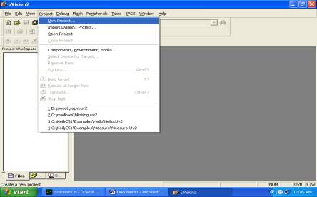
- Save the Project by typing suitable project name with no extension in u r own folder sited in either C: or D:
- Then Click on Save button above.
- Select the component for u r project. i.e. Atmel……
- Click on the + Symbol beside of Atmel
- Select AT89C51 as shown below
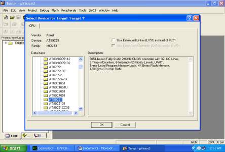
- Then Click on “OK”
- The Following fig will appear
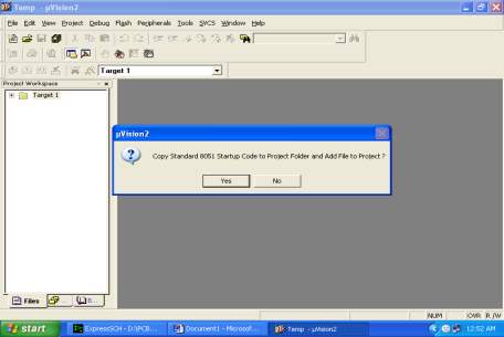
- Then Click either YES or NO………mostly “NO”
- Now your project is ready to USE
- Now double click on the Target1, you would get another option “Source group 1” as shown in next page.
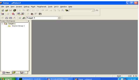
- Click on the file option from menu bar and select “new”
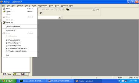
- The next screen will be as shown in next page, and just maximize it by double clicking on its blue boarder.
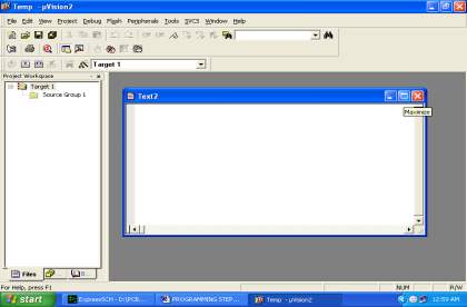
- Now start writing program in either in “C” or “ASM”
- For a program written in Assembly, then save it with extension “. asm” and for “C” based program save it with extension “ .C”
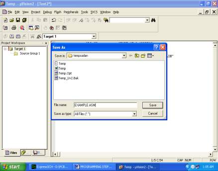
- Now right click on Source group 1 and click on “Add files to Group Source”
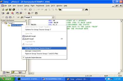
- Now you will get another window, on which by default “C” files will appear.
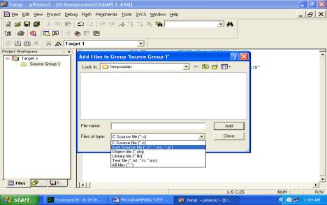
- Now select as per your file extension given while saving the file
- Click only one time on option “ADD”
- Now Press function key F7 to compile. Any error will appear if so happen.
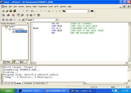
- If the file contains no error, then press Control+F5 simultaneously.
- The new window is as follows
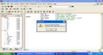
- Then Click “OK”
- Now Click on the Peripherals from menu bar, and check your required port as shown in fig below
- Drag the port a side and click in the program file.
- Now keep Pressing function key “F11” slowly and observe.
- You are running your program successfully
5.2 PROLOAD:
Proload is software which accepts only hex files. Once the machine code is converted into hex code, that hex code has to be dumped into the microcontroller and this is done by the Proload. Proload is a programmer which itself contains a microcontroller in it other than the one which is to be programmed. This microcontroller has a program in it written in such a way that it accepts the hex file from the Keil compiler and dumps this hex file into the microcontroller which is to be programmed. As the Proload programmer kit requires power supply to be operated, this power supply is given from the power supply circuit designed above. It should be noted that this programmer kit contains a power supply section in the board itself but in order to switch on that power supply, a source is required. Thus this is accomplished from the power supply board with an output of 12volts.
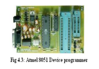
Figure 5.1 ATMEL 8051 Device programmer
5.2.1 Features:
- Supports major Atmel 89 series devices
- Auto Identify connected hardware and devices
- Error checking and verification in-built
- Lock of programs in chip supported to prevent program copying
- 20 and 40 pin ZIF socket on-board
- Auto Erase before writing and Auto Verify after writing
- Informative status bar and access to latest programmed file
- Simple and Easy to use
- Works on 57600 speed
5.2.2 Description:
It is simple to use and low cost, yet powerful flash microcontroller programmer for the Atmel 89 series. It will Program, Read and Verify Code Data, Write Lock Bits, Erase and Blank Check. All fuse and lock bits are programmable. This programmer has intelligent onboard firmware and connects to the serial port. It can be used with any type of computer and requires no special hardware. All that is needed is a serial communication ports which all computers have.
All devices have signature bytes that the programmer reads to automatically identify the chip. No need to select the device type, just plug it in and go! All devices also have a number of lock bits to provide various levels of software and programming protection. These lock bits are fully programmable using this programmer. Lock bits are useful to protect the program to be read back from microcontroller only allowing erase to reprogram the microcontroller. The programmer connects to a host computer using a standard RS232 serial port. All the programming ‘intelligence’ is built into the programmer so you do not need any special hardware to run it. Programmer comes with window based software for easy programming of the devices.
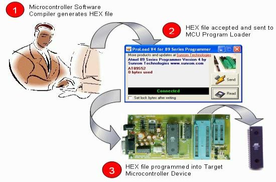
5.2.3. Programming Software:
Computer side software called ‘Proload V4.1’ is executed that accepts the Intel HEX format file generated from compiler to be sent to target microcontroller. It auto detects the hardware connected to the serial port. It also auto detects the chip inserted and bytes used. Software is developed in Delphi 7 and requires no overhead of any external DLL.
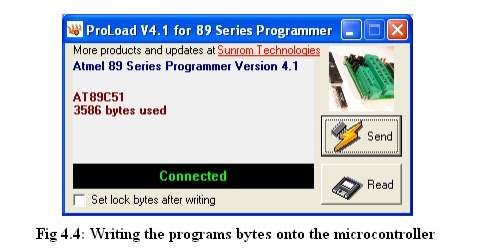
CHAPTER 6
PROJECT IMPLEMENTATION
6.1 SCHEMATIC DIAGRAM
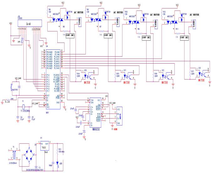
Figure 6.1 Schematic diagram
6.2 WORKING
The thought behind this project is to utilize the current GSM foundation. In this way, every one of the operations include the GSM framework too. As we send any sms, it experiences the GSM framework. Any sent sms can be gotten in the event that we utilize a SIM card and GSM module. To work any GSM modem, we need to utilize the AT orders to work them. For instance, if any sms arrives the GSM modem sends the serial information in ASCII organize. We can read these information on the off chance that we associate the modem with the serial port of the microcontroller at the baud rate of 9600. As the microcontroller comes to realize that a sms has been arrived, it can sent an appropriate AT summon to peruse the sms.
The perusing of sms returns the versatile no of sender, the time and a great deal more data. We need to choose the sms part of the message. The beginning string of the sms is utilized as the secret word. As the secret key is coordinated, then the sms entry is thought to be legitimate by the microcontroller else, it overlooks the sms. Working of “sms based gadget control framework utilizing GSM MODEM” is extremely basic. It can be essentially comprehended by its square chart &circuit graph.
The GSM modem will be interfaced to the microcontroller area through serial port interface. On the off chance that the client needs to work the lights and different machines, he can simply send a predefined message to the GSM modem that is interfaced to the controller area. The controller segment will have the switch controls of the gadgets. Every one of the lights and apparatuses which are to be controlled will be associated with the controlling gadget i.e., to the microcontroller area. The microcontroller consequently, makes an impression on the versatile number about the status of the considerable number of lights. At controlling side we have GSM modem with one SIM, small scale controller, apparatuses controlling circuit, status recognizing criticism framework. The client needs to send a predefined SMS to the telephone number which is embedded in modem, then modem will demonstrate this new message to controller. Controller will read this message and control the lights as indicated by message it got. This framework additionally identifies light disappointment condition and shows this data on LCD and sends a SMS to the portable.
CHAPTER 7
RESULTS AND DISCUSSION
7.1. IMPLEMENTATION RESULTS
During the power on software initializes the LCD(P0 Pins) in 4 bit mode, Load output Pins, Load Feedback input Pins, GSM Module Connected to UART Pins.After LCD Initialization happens it updates the Operations data on to the LCD screen.
To initialize the GSM mode it requires the SIM card or else it displays GSM Initialization error on the LCD screen and re-initialises the GSM until it initializes in the proper way.
The following messages has to send to turn ON the Load and off the same.
Message for Load 1 ON: 100
Message for Load 2 ON: 010
If system fails to ON the Load, it gives the feedback SMS to Owner for respective load.
Hardware uses the voltage level shifters and Triac switches to handle the load voltages up to 230v AC for control and feedback since AT89s52 capable of only 5v and 20 mA current.
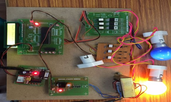
Figure 7.1. Project Results
7.2 ADVANTAGES
- Gadgets can be controlled from long distances.
- Conservative plan
- Can be effortlessly actualized in homes
- Can be utilized by everybody with simply the information of content SMS
- Organization of the SMS is easy to comprehend and compose.
7.3 DISADVANTAGES
1. The system is network dependent. Hence, network congestion can reduce the 00 reliability of the system.
2. User can make mistake while typing the message format.
CHAPTER 8
CONCLUSION AND FUTURE SCOPE
8.1 CONCLUSION
The project we have attempted has helped us pick up a superior viewpoint on different perspectives identified with our course of study and additionally functional information of electronic types of gear and correspondence. We got comfortable with programming examination, outlining, execution, testing and support worried with our venture.
The broad abilities of this framework are what make it so fascinating. From the accommodation of a straightforward mobile phone, a client can control and screen essentially any electrical gadgets. This makes it workable for clients to rest guaranteed that their assets are secure and that the TV and other electrical machines was not gone out to simply list a couple of the many employments of this framework.
The final result will have a shortsighted plan making it simple for clients to collaborate with. This will be basic due to the extensive variety of specialized information that property holders have.
8.2. FUTURE SCOPE
The future implications of the project are extremely incredible considering the measure of time and assets it spares. The viable uses of this venture are tremendous and can have incomprehensible level of usage. This little idea can be utilized as a part of fields, for example, climate estimating, remote detecting, apply autonomy, flying, home robotization, and numerous other related fields where nonstop checking and direction is required. So this is not the finish of the venture yet rather is a stage towards investigating different potential outcomes that it carries with it.
The project itself can be adjusted to accomplish a total Home Automation System which will then make a stage for the client to interface amongst himself and his family.
REFERENCES
- Mazidi, Muhammad ali, The 8051 Microcontroller and Embedded Systems,Second Edition, Prentice Hall, 2007
- Mouly, M., and M. B. Pautet, The Global System for Mobile Communications, 1993.
- Wikipedia-GSM technology
- 8051 microcontrollers: an applications-based introduction
- http://elprojects.blogspot.in/2010/03/lcd-pin-description-for-interfacing.html
- www.google.com
- www.keil.com
Cite This Work
To export a reference to this article please select a referencing stye below:
Related Services
View all


Related Content
All TagsContent relating to: "Technology"
Technology can be described as the use of scientific and advanced knowledge to meet the requirements of humans. Technology is continuously developing, and is used in almost all aspects of life.
Related Articles

DMCA / Removal Request
If you are the original writer of this dissertation and no longer wish to have your work published on the UKDiss.com website then please: