Design and Construction of Class AB Audio Amplifier
Info: 7229 words (29 pages) Dissertation
Published: 1st Nov 2021
Abstract
For an excessive period, Class A and Class AB were the only amplifier classes that are compatible with high quality audio systems. This is because valves were the single active device, and Class B amplifiers generated masses of distortion which made them barely acceptable for numerous purposes. Construction of Class AB amplifiers are initiated to overcome zero crossing distortion in Class B amplifiers commonly called as Crossover Distortion. In order to develop an amplifier with the low distortion of the Class A configuration along with the high efficiency output of Class B configuration is to build an amplifier circuit which is a combination of the previous two classes resulting in an advanced type of amplifier called Class AB amplifier.
This paper describes the design and the construction of the Class AB audio amplifier. A proposed approach is outlined and the challenges encountered during developing a well-designed circuit in this project are addressed in this report [10]. Though the amplifier is unsuccessfully functioning at the end of the project, masses of knowledge and skills are attained throughout the Semester 1 and Semester 2. For example, basic skills on methods of using the laboratory instruments such as the oscilloscope, multi meter, signal generator,etc, and designing and simulating circuits on multiple simulation programs such as LTSpice, PSpice, etc. Knowledge on reading schematic circuits and constructing a simple circuit on breadboard are also obtained.
Table of Contents
1 Introduction
2 Industrial Relevance
3 Theoretical Background
4 Design
5 Experimental Method
6 Results and Discussion
7 Conclusions
Reference List
Appendices
List of Figures
Figure 1‑1: Block Diagram of a Power Amplifier…………………….
Figure 1‑2: Efficiency of Amplifier Classes…………………………
Figure 1‑3: Output Waveform of Class AB…………………………
Figure 1‑4: Basic Operation of Class AB Amplifier…………………..
Figure 2‑1: A head unit……………………………………….
Figure 2‑2: In-trunk unit………………………………………
Figure 2‑3: Location of active noise cancellation……………………
Figure 2‑4: Process of active noise cancellation…………………….
Figure 2‑5: A typical home theater system………………………..
Figure 2‑6: SR system commonly used in live performances…………..
Figure 2‑7: PA system equipment……………………………….
Figure 2‑8: Portable and home docking station…………………….
Figure 3‑1: Crossover Distortion in Class B Amplifier…………………
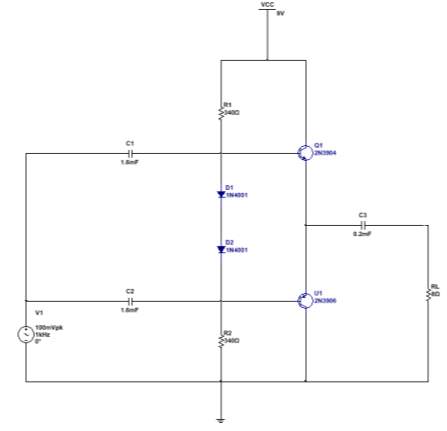
Figure 4‑1: Class AB amplifier with Resistor Biasing…………………
Figure 4‑2:Class AB Q-Point Cutoff………………………………
Figure 4‑3: Class AB amplifier with diode biasing……………………
Figure 4‑4: LTSpice simulation of the output signal………………….
Figure 6‑1: LTSpice Simulation of reference current, Iref……………..
Figure 6‑2: LTSpice simulation of positive and negative side waveform signal
Figure 6‑3: LTSpice simulation of audio input signal against output signal..
List of Tables
Table 1: Classes of Amplifiers…………………………………………
1 Introduction
This report covers the fields of Analogue Electronics and Technological Plasmas. The main purpose of the project is to design and build a power amplifier which is built using high power semiconductors in Class AB topology. The amplifier is incorporated with a speaker as the output. The circuit involves a combination of Class A and Class B power amplifiers with a biasing stage connected at the base of the complementary transistors. The transistors are barely turned on by means of biasing the base of NPN and PNP transistors with enough voltage. There are several biasing techniques available to achieve the most efficient amplifier which is briefly discussed later. Failed attempts and problems encountered during phases of the project are addressed in this report.
1.1 Power Amplifiers
At least a single amplifier is implemented in nearly all electronic devices today regardless of the existence of several classes of amplifiers. Amplifiers are classified by their function which implies whether the device is a voltage amplifier or power amplifier, and its frequency response characteristics. The working description of an amplifier is acknowledged on the condition that the function and frequency response classifications are established. Nevertheless, each type of amplifiers is not described. This report is mainly concentrated on Class AB amplifiers topology. Class AB are largely favored as audio power amplifiers. Power amplifiers are large signal amplifiers. Generally, the output signal power of an amplifier is enhanced when compared to the input signal power. Vast majority of power amplifiers are commonly fitted as the final stage of amplification to drive a loudspeaker load.
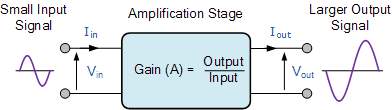
Figure 1‑1: Block Diagram of a Power Amplifier
1.2 Classification of Amplifiers
Amplifier classes are denoted by the sum of output signal diverges within the amplifier circuit throughout one cycle of process once presented by sinusoidal input signal. The classification of amplifiers is solely varied base on their linear operation but with far greater efficiency, whilst the rest are a compromise between linearity and efficiency. Amplifiers are primarily grouped into two classes. The first are the classically organised conduction angle amplifiers developing the usual amplifier classes of A, B, AB and C, which are described by the span of their position of conduction over certain ration of the output waveform, such that the output stage transistor operation lies someplace within being saturated and cut off. Digital circuits and pulse width modulation (PWM) are utilised in the second group of amplifiers to continuously shift the input waveform between “fully-ON” and “fully-OFF” which leads the output waveform firmly into the transistors saturation and cut off regions. These latest “switching” amplifiers consist of class D, E, F, G, S, and T.
Class A, B, C, and AB amplifiers are predominantly built as audio amplifiers when compared to the second group of switching amplifiers. Figure 1-1 below shows the four type of amplifiers and its efficiency. Every class of operation has certain usages and features. No class of operation is superior than any other class. The choice of the finest class of operation is decided by means of amplifying circuit depending on the target application. For example, the greatest class of operation for a turntable may not be the greatest class for a radio transmitter.
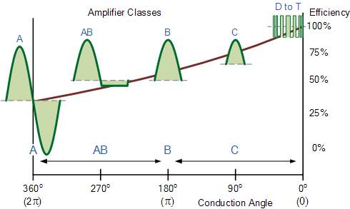
Figure 1‑2: Efficiency of Amplifier Classes
These amplifiers vary from a near linear output with low efficiency to a non-linear output with a high efficiency. The characteristics of each type of amplifier are summarised in Table 1-1 below;
Table 1‑1: Classifications of Amplifiers
| Class | A | B | C | AB |
| Conduction Angle | 360 | 180 | Less than 90 | 180 to 360 |
| Position of the Q point | Centre Point of the Load Line | Exactly on the X-axis | Below the X-axis | In between the X-axis and the Centre Load Line |
| Overall Efficiency | Poor
25% – 30% |
Better
70% – 80% |
Greater than 80% | Greater than A but less than B 50% – 70% |
| Signal Distortion | None if properly biased | At the X-axis Crossover Point | Large | Small |
1.3 Class AB Amplifier Operation
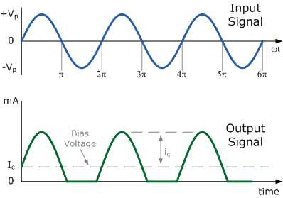
Figure 1‑3: Output Waveform of Class AB
As mentioned in previous section, Class AB is not legitimately a separate class of its own, but a combination of Class A and B. The Class AB amplifier output stage incorporates the advantages of the Class A and the Class B amplifier while reducing the problems of low efficiency and distortion correlated with them. Class A is well-known for having the highest linearity out of all other classes of amplifiers and its operation denotes that the collector current never cut off for any portion of the cycle. It has a transistor which is biased with voltage to ensure that it stays on all the time. This single transistor operates both positive and negative waveform.
On the other hand, a Class B amplifier was created as the key solution to the heating and efficiency complications linked with the preceding class A amplifier. The operation of a Class B transistor amplifier implies that the collector current is cut off for one-half cycle (180 degree), on either side of waveform cycle of the input signal. Class B is a push-pull type amplifier which uses two transistors. The NPN transistor is turned on at the positive side and is turned off at negative side. In contradiction, the PNP transistor is turned on at negative side and turn off at positive side. At crossover point of zero value, distortion occurs. The reason for this is because nothing up to 0.7V is being turned on, thus neither transistors turns on until it goes greater than 0.7V either on positive or negative side to get bipolar transistor to start conducting. In order to overcome this zero-crossing distortion in Class B amplifiers commonly recognized as Crossover Distortion, Class AB is introduced [10].
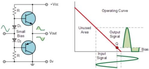
Figure 1‑4: Basic Operation of Class AB Amplifier
Presently, Class AB is undeniably the utmost common amplifier class used in home stereo and similar amplifiers. It generates the outstanding sound quality of the Class A topology with the high efficiency of the Class B. Figure 1-3 and 1-4 explains its basic operation. Class AB use a pair of transistors; both being biased slightly ON ensuring that the distortion complications around the crossover point associated with previous Class B amps is mostly eliminated. The transistors do not go into its full off range. This is achieved by implementing two diodes in the circuit. With AB amplifiers, distortion is worst when the signal is at its minimum value. Paradoxically, the distortion is at its lowest when the signal reaches it clipping point. When Class AB receive their side of the waveform they will enter its full saturation, turn on and conduct, resulting the output comes out the speaker [10].
2 Industrial Relevance
2.1 Market Analysis
The industrial relevance of this project is vast, and numerous beneficial results are predicted. Nowadays, audio power amplifiers are economically noteworthy and essentially a commodity. The evolution of amplifiers has a history extending back to the 1920s [2]. Expectations in this invention are progressing over the decades. Higher power, lighter weight, cleaner sound, less heat and increased reliability, all for less cost and less weight per watt [11]. They are commonly utilized in the consumer electronic devices such as high fidelity (hi-fi) audio players, a smartphone and a tablet.
Class AB amplifiers predominantly monopolise the trade of audio power amplifiers since it offers adequate compromise between linearity and efficiency and they emulate the finest Class A amplifiers in sound quality. Despite the fact Class A amplifiers are the least practical and cost the most, they do possess the finest sound. Concurrently, Class AB have less power usage than Class A, inexpensive, and can be lighter, cooler and smaller. Theoretical maximum efficiency of this amplifier class is roughly around 78.5% and possess a much better ratio than the 25% theoretical maximum efficiency of Class A amplifiers. The “real world” maximum efficiency is likely to be around 70% and is influenced by the output stage topology and output stage biasing. Under typical listening conditions (around 30% of full power), the amplifier power efficiency will be around 35% [12]
Growing technology and high adoption rate of these high-end products worldwide are dominating the market of power amplifier. The intended audience for this market are mostly amplifiers manufacturers, amplifiers suppliers, smartphone manufacturers and distributors, manufacturing companies, consumer electronic product manufacturers and suppliers, and finally audiophiles, the consumer of electronic products themselves. Global Power Amplifier Market has been valued at USD976 million in the year 2015 which is increasing with compound annual growth rate (CAGR) of 16% from 2016 to 2022 and estimated to expand at USD2.8 billion by end of forecast period [21]. In the meantime, Asia-Pacific is driving the marketplace with total share of 63%. Rising economy of Asian countries such as China and India including solid presence of manufacturing industry in China and Indonesia regions are upholding the power amplifiers industry as well [21].
2.2 Target Applications
Applications of this high-performance device in the expansive electronic industry today is boundless. Contributions made by Class AB amplifiers for each target application is briefly explained below;
2.2.1 Automotive head and in-trunk units
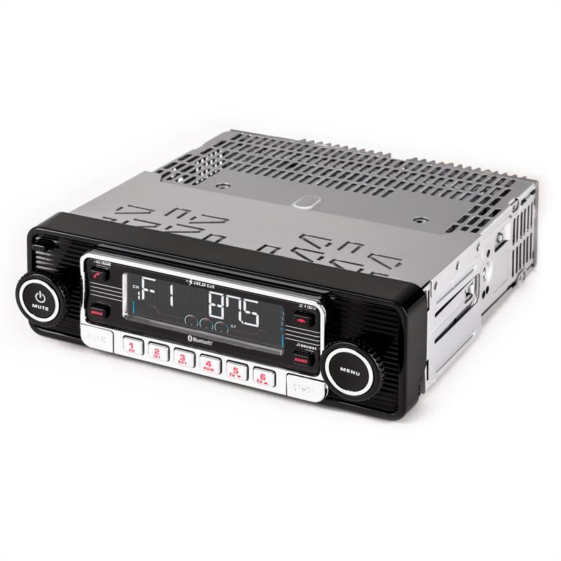
Figure 2‑1: A head unit
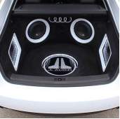
Figure 2‑2: In-trunk unit
Class AB amplifiers offer best-in-class performance vastly in auto parts primarily for car radio (head units) and multi-channel sound systems (in-trunk unit). These parts are usually traded by original equipment manufacturers (OEM) and automotive aftermarket. In the United States, online sales and aftermarket automotive accessories have exhibited an upsurge in their year over year (YOY) results over conventional brick and mortar stores. In fact, per Hedges & Company, “Sales of auto parts and accessories continued to climb in 2016, and will continue the trend into 2017 to reach USD8.9 billion dollars, posting around a 16% increase over 2016 [20].
2.2.2 Automotive active noise cancellation
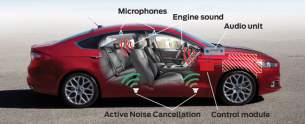
Figure 2‑3: Location of active noise cancellation
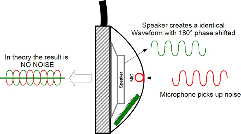
Figure 2‑4: Process of active noise cancellation
Active Noise Cancellation (ANC) is invented to effectively diminish low frequency noise in a car’s interior. Regardless of whether the audio unit is being turned on or off, the operation of the system will be intact on any occasion the automobile is running [23].
Low-end drivetrain (system in a vehicle which joins the transmission to the drive axles) frequencies entering the interior are captured by the two microphones in the cabin area and a signal is transmitted to the ANC unit. A precisely timed reversed phase audio signal is generated by the control unit afterwards, before being delivered to the amplifier. The door speakers and the subwoofer located on the rear parcel shelf are being powered by the amplifier. Subsequently, a remarkable decline in exterior noise level such as the engine sound is resulted.
2.2.3 Home theater system
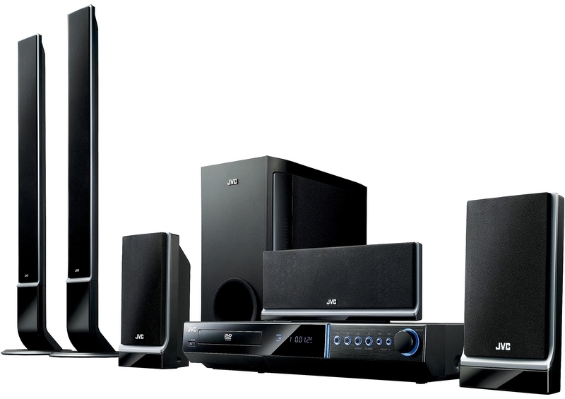
Figure 2‑5: A typical home theater system
Home theater is an entertainment system which consist of a combination of any type of television with video components and audio system offering surround sound with numerous speakers. Home theaters are usually built to imitate the quality of viewing media in the cinema and intended for majority of people who evidently prefer playing their video games and tunes, and watching their favorite films, television shows and series in the comfort of their own private residences today. The cost of home theater installation consisting of a LED television, cable service and audio setup is estimated to have a minimum value of USD199 and is averaged about USD1 300 depending on consumer needs. Conversely, a premium system with TV calibration, custom furniture, audio setup, and speakers stands, among other things, can cost up to USD16 500.
2.2.4 Sound reinforcement (SR) system
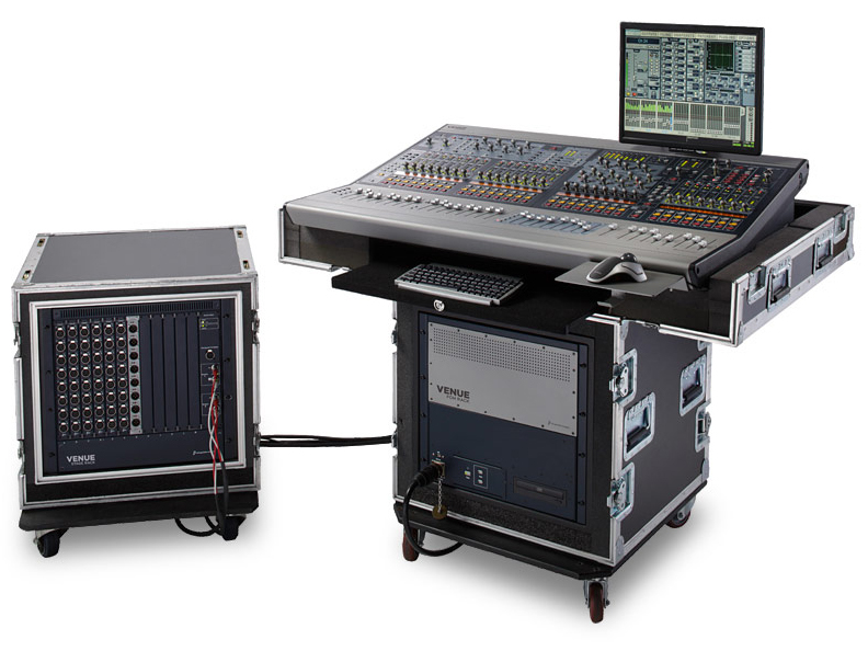
Figure 2‑6: SR system commonly used in live performances
An arrangement of microphones, signal processors, amplifiers, and loudspeakers installed altogether in speaker cabinets is called a sound reinforcement system. The SR system is powered and managed by an audio mixing board which enhances and modify sounds, makes live or pre-recorded sounds louder and clearer and is vastly utilized during huge concerts and live performances to circulate those sounds to a bigger or further isolated or far audience. For example, one people speaking on a stage may not be heard well at the back of a large hall. A sound system may be used to make the sound more clearly audible and assist people’s hearing abilities. In this case, the intention is to create the voice at the back of the hall sound as loud as (not louder than) it is when heard up close. For artistic purposes, amplification by a sound system delivers audience with grander musical impact by making it appear “larger than life”.
2.2.5 Public address (PA) system
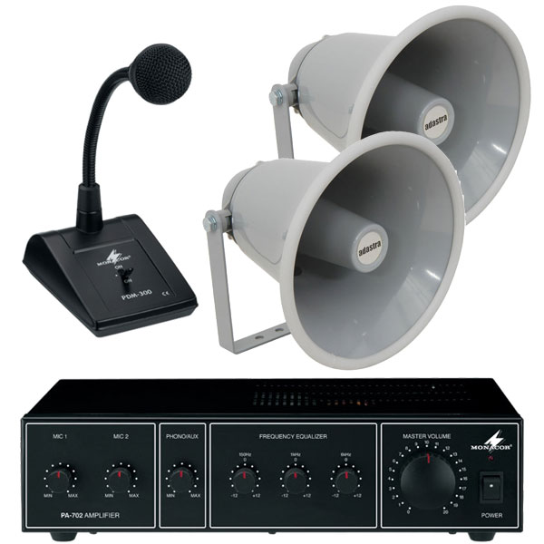
Figure 2‑7: PA system equipment
Public Address (PA) system consents one person communicate to a crowd of people and is broadly exploited to make announcements in public, institutional and commercial buildings and locations, for example universities, churches, sports arenas and huge passenger airplanes. PA system facilitate people to hear sounds in isolated places such as seminars or meetings which sometimes draw larger crowds than the capacity of the meeting room. Therefore, the excess crowd can hear speeches and discussion delivered to a second room. Sound reinforcement system and public address system may use certain identical components, but with divergent target applications. SR system are intended for live arts or music performance, whereas PA system are primarily for reproduction of speech.
2.2.6 Portable and home docking stations
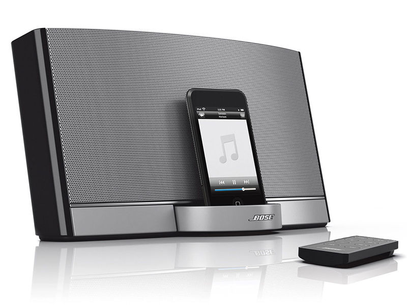
Figure 2‑8: Portable and home docking station
An audio docking station is an ideal choice for audiophiles to play their digital music collection as it accommodates electronic devices such as smartphones, iPods, and mp3 players to playback music, apart from charging the device’s battery. A basic standalone docking station is inexpensive when compared to their equivalents making them a supreme choice for people on a budget with prices ranging from as minimum as £10 leading up to £40. Accordingly, they are often perfect for travelling, or for individuals who wants to listen to music outside as they are incline to have high portability, and battery power or Bluetooth selection. Meanwhile, the combined docks can range from £20 all the way up to over £200. Currently, the timeworn bulky Hi-Fi theater systems are being replaced gradually by this handy product in household due to their lightness, miniature size and multiple features.
With the ever-growing demands and performance desires in the audio market, there are many other target applications available and have been countless advancements in audio amplifier topologies [10]. As with all audio systems, huge attentiveness at all aspects regarding Class AB amplifiers is required to obtain unsurpassed system performance. It is highly improbable for hi-fi enthusiasts to vanish in the future since they are indeed the existing fraternity who are prone to invest substantially in making a distinctive experience in their home, workplace or automobiles. Consequently, familiarity regarding the classes of audio amplifiers accessible in the market and the features linked with every one of them is crucial in selecting the finest audio amplifier for proper application [18, 10].
3 Theoretical Background
In this chapter, the architecture of a basic Class AB power amplifier is explained in details. Several materials regarding transistors are initially discussed, and a straightforward analysis of the building block fundamentals which are unavoidably implemented in the construction of an entire amplifier circuit is followed. Successively, a solid foundation for the comprehensive study of the simple amplifier that trails is provided. Chapter 4 then leads to the journey of the amplifier construction, where the design is evolved and assessed as its performance is enhanced. The design considerations are vital in ensuring unsurpassed performance of the amplifier. The primary performance specifications are discussed below;
3.1 Power Output
Every single output device has its limit of endurance towards thermal dissipation. This limit point when the device is incapable to sustain heat is identified as the output power. Maximum output power is commonly estimated for a load of 8 and 4 loudspeakers which are frequently used in hi-fi applications. Twice amount of current flow is generated when a specific voltage is applied to 4 load. Consequently, the output power is doubled as well.
3.2 Bipolar Junction Transistor (BJT)


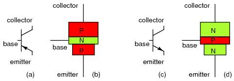
Figure 3‑1: Bipolar Junction Transistors
The utmost vital illustration of an active component is a transistor. This device amplifies and generates an output signal with superior power than in the input signal. The additional power comes from an external source of power supply. The key ingredient of nearly all audio power amplifiers in the market today is the bipolar junction transistor (BJT). Adequate knowledge regarding the characteristics of transistor amplifier circuits and its limitations are briefly explained in this section.
3.3 Crossover distortion
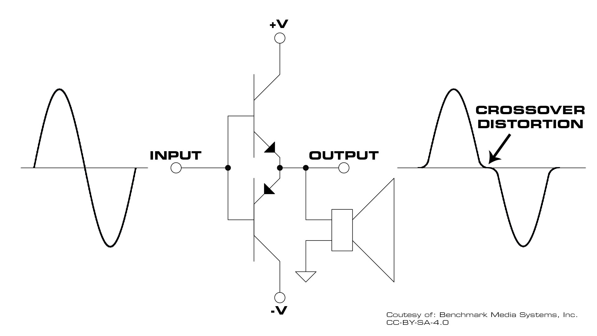
Figure 3‑2: Crossover Distortion in Class B Amplifier
The complementary NPN and PNP transistors are turned off whenever the DC base voltage becomes zero. Concurrently, the input signal voltage is required to surpass base emitter voltage, VBE before either transistor takes turn to conduct its positive and negative cycle waveform subsequently. The main reason this distortion commonly occurs in Class B amplifier is because of the time gap existence among the positive and negative cycles waveform of the input signal every time the transistors are off as shown in Figure 3-1 above. Crossover distortion is resulted because of this occurrence.
3.4 Class AB Amplifier Biasing
In pursuance of eliminating crossover distortion, Class AB amplifier is introduced and the biasing is adjusted to exceed the base emitter voltage, VBE of the complementary transistors in this type of amplifier. Class AB amplifier is built by biasing the voltage of both switching transistors into slight conduction in an ordinary Class B push-pull stage amplifier, regardless of whether input signal is present. The conduction of both transistors simultaneously is guaranteed by the minimal biasing arrangement. The 0.6 to 0.7V dead band which is created during the occurrence of crossover distortion in Class B amplifiers is significantly lowered by applying acceptable biasing. Several methods of pre-biasing the transistor devices are available such as implementing a voltage divider network, a current mirror (a series connected diode arrangement) and a preset voltage bias. Thus, Class AB amplifier is concluded basically as a Class B amplifier with “Bias”.
A straightforward biasing approach are diode-connected transistors identical to NPN and PNP transistors. They form mirrors with the quiescent currents, IQ set by matched resistors, which is commonly called as a Current mirror. In this circuit arrangement, both diode and transistor emitter-base junction’s characteristics are closely matched, thus equal current in diodes and transistor. In bias path both resistors are the same value.
4 Design
The design considerations of the Class AB amplifier are discussed here. Research analysis is performed and several favorable circuit designs are selected.
4.1 Resistor Biasing
Based on Figure below, a pair of complementary (NPN and PNP) transistors is employed in the circuit design. The transistors chosen are the 2N3904 NPN with maximum collector-emitter voltage, VCEO of 40 V and 2N3906 PNP with similar maximum VCEO value of 40 V. This circuit is powered with a supply voltage, VCC of 9V and the speaker impedance, ZL is 8. The NPN transistor is biased slightly above its 0.7 V barrier potential by R1 and R2 resistors. The PNP transistor is biased by R3 and R4 resistors correspondingly as the NPN transistor. Resistors R1, R2, R3, and R4 are identified as biasing resistors and resistor RL is the load resistor with the value of 1 k. The input coupling capacitors C2 and C3 including the output coupling capacitor C4 are implemented in this design. Several circuit simulations are performed and the output signal waveform obtained is displayed below;
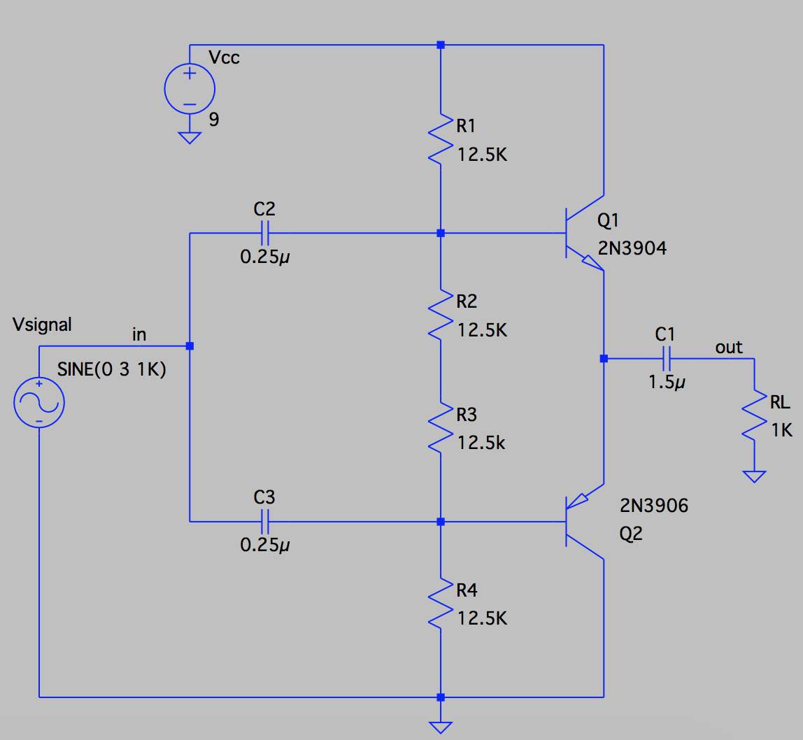
Figure 4‑1: Class AB amplifier with Resistor Biasing
4.1.1 Operation Point
Base-emitter junction of the two complementary transistors are slightly forward biased. Quiescent point is expected to locate marginally above the VCE cut-off. The Q point is illustrated in Figure 3-1 below.
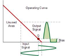
Figure 4‑2:Class AB Q-Point Cutoff
The value of Q point voltage, VCEQ is halved the power supply, VCC. The saturation current, IC(sat) is calculated by dividing VCEQ with RL. The transistors are forward biased with Q point current, ICQ which is estimated to be between 1% to 5% of IC(sat).
4.1.2 Biasing Resistors
Based on the circuit in Figure, the resistor values are obtained by performing calculations as below;
Assume R=R1=R2=R3=R4,
2×Ibias×R= VCC
Where
R= VCC2×Ibias
Since Ibias = ICQ,
R= VCC2×ICQ
R= 0.25×VCCICQ
Assume ICQ = 0.04IC(sat), then
R= 0.25×VCC0.04×IC(sat)
Since VCEQ = VCC/2 and IC(sat) = VCEQ/RL,
IC(sat)= VCC2×RL
Substitute IC(sat) in equation R, to get
IC(sat)= 0.25×2×RL0.04
Since RL = 1 k, then
R= 0.5×10000.04=12 500 =12.5 k
So, R1=R2=R3=R4=12.5 k
The biasing resistors value is obtained to overcome the 0.7 V barrier potential. Subsequently, the input and output coupling resistors are added. This is to ensure the flow of 1 kHz input signal from the base of transistors to amplifier stage and finally reaches the output stage, RL.
4.1.3 Input Power
The formula for AC input power, Pin;
Pin= Vin(peak-peak)2ZL×Zin(stage)
The positive cycle waveform NPN transistor, Zin(stage) is;
Zinstage= R1||R2|| Zinbase
Where
Zin(base)= β×RL
Zin(base)= 170×1 k =170 k
Hence
Zin(stage)= 12.5 k||12.5 k||170 k=6 k
Since there are two NPN and PNP input stages,
Zin EQ(stage)=Zin(stage)2=6 k2=3 k
Substitute Vin= 2 V, Zin EQ(stage)= 3 k and ZL= 8 into equation input power, Pin, to get
Pin=Vin(peak-peak)2ZL×Zin(stage)= 228×3 k=0.16 mW
4.1.4 Output Power
The formula for AC output power, Pout;
Pout= Vout(peak-peak)2ZL×RL228×1 k=0.5 mW
4.1.5 Power Gain
The formula for power gain, AP;
AP= PoutPin=0.5 m0.16 m=3
4.1.6 Maximum output power
The formula for maximum output power, Pout(max);
Pout(max)= VCC2ZL×RL=928×1 k=10 mW
4.1.7 Power Efficiency
The formula for power efficiency, ;
Efficiency, η= Pout(max)PDC×100%
The value of DC power, PDC;
PDC= VCC×IDC
Where
IDC= Ibias+IC(sat)π
IDC= Ibias+IC(sat)π
Substitute IC(sat)= VCC/(2RL) into equation IDC, to get
IDC= Ibias+VCC2×RL×π=0.18 m+92×1 k×π=0.18 m+1.43 m=1.61 mA
Hence,
PDC= 9×1.61 m=14.5 mW
Since maximum output power, Pout(max)=10 mW, and PDC=14.5 mW, thus
Efficiency,η= Pout(max)PDC×100%=Efficiency= 10 m14.5 m×100%=68.96%
Using all the calculations above, the Class AB amplifier is designed and advanced to the production stage.
4.2 Class AB amplifier with biasing diodes
Based on Figure below, a pair of diodes is replaced in the circuit as an improvement and a more suitable alternative than two simple resistors as the biasing stage. Diodes generally cope better with the variation of temperature when the complementary transistors are biased marginally beyond the cut-off region.

1N4148
1N4148
Figure 4‑3: Class AB amplifier with diode biasing
The circuit diagram above shows similarities from previous design arrangement with complementary NPN 2N3904 and PNP 2N3906 transistors. However, the biasing stage is replaced with the two commonly used small signal fast switching 1N4448 diodes. These diodes are connected in series along with the two biasing resistors R1 and R4. The output stage is fitted with a load resistor, RL of 8 . An AC signal of 1 kHz with 100 mVpeak-peak is connected which is provided by the signal generator available in the lab.
R1 and R4 resistors are calculated to establish the appropriate value for biasing the transistors. Calculations should be simpler if both resistors are assumed to have equal values.
4.2.1 Biasing resistors
Assume R= R1=R4, then
VCC=(2×RIbias)+(2×VBE)
R=VCC-(2×VBE)2×Ibias
Where the biasing current, Ibias flowing across the diodes and resistors is equal to ICQ (the Q point collector current) and base-emitter voltage, VBE of a transistor is 0.7 V.
In this case, two resistors and two transistors are available. The crossover distortion commonly occurs in Class B amplifier is diminished by adjusting the ICQ roughly around 1% to 5% of IC(sat).
Assume Ibias=ICQ=0.02IC(sat), where IC(sat) = VCC/(2RL)
Substitute VCC=9 V and RL=8 into equation IC(sat) to get
IC(sat)=VCC2×RL=92×8=0.56 A
If IC(sat) =0.56 A, then
Ibias=ICQ=0.02×IC(sat)=0.02×0.56=11.2 mA
Hence
R1=R4=R=VCC-(2×VBE)2×Ibias=9-(2×0.7)2×11.2 m=7.622.4 m=340
The amplifier design is placed with both 340 resistors. The input and output coupling capacitors values are estimated by determining the values of the input impedance, ZIN and output impedance, ZOUT. The presence of crossover distortion in the output signal is observed by connecting the amplifier to the oscilloscope. The display screen of the instrument is shown in Figure 3-4 below;
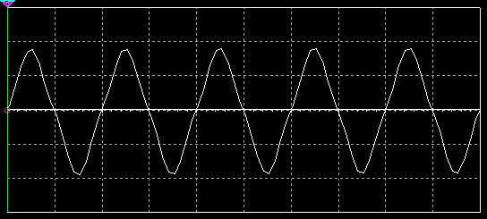
Figure 4‑4: LTSpice simulation of the output signal
5 Experimental Method
To accomplish expected results, several approaches are performed. Instrument and materials required in the circuit design and tests are specified in this chapter.
Laboratory Instrument and Electronic Components required:
- Power Supply
- Digital Multimeter
- Function Signal Generator
- Oscilloscope
- Breadboard
- Crocodile Clips
- Wire Jumpers
- 8 Speaker
- Heat Sink
- 1N4148 Diodes
- 1 NPN Q2N3904 Transistor
- 1 PNP Q2N3906 Transistor
- Multiple value resistors
- Multiple value capacitors
Procedure:
6 Results and Discussion
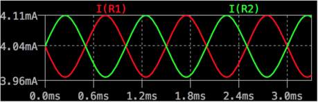
Figure 6‑1: LTSpice Simulation of reference current, Iref
Figure 6-1 above demonstrates the base-emitter voltage. VBE of NPN transistor (positive half cycle) and PNP transistor (negative half cycle) is respectively 0.7V.
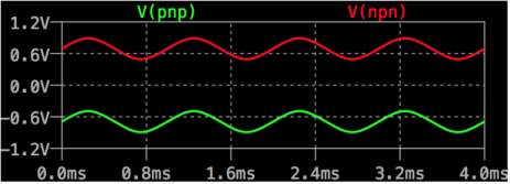
Figure 6‑2: LTSpice simulation of positive and negative side waveform signal
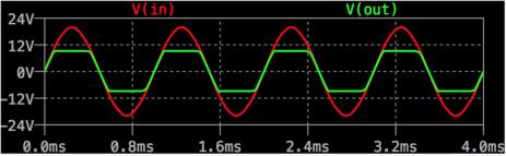
Figure 6‑3: LTSpice simulation of audio input signal against output signal
Amplification of signal is unsuccessful based on Figure 6-3 above. Clipping is shown and no audio output is heard when connected to 8 speaker.
7 Conclusions
Survey regarding various classes of audio amplifiers frequently used in designs today is briefly described in this report. In pursuance of developing an amplifier with low distortion of the Class A configuration along with the high efficiency output of Class B configuration is to build an amplifier circuit which is a combination of the previous two classes. Many circuit stimulations are performed using PSpice and LTSpice program to estimate output of several circuit designs. In this project, the amplifier is unsuccessfully functioning. Expected results are not achieved and tallied with circuit simulations on LT Spice. No audio output is heard when the amplifier is connected to the speaker with 8 impedance. Initially, the project is estimated to progress efficiently per schedule. However, a few unexpected challenges and delays are encountered during different phases of the project. Lack of understanding on the basic principles of transistors, Class AB topology including proper use of basic lab instruments are the core causes of project failure. Lots of time are misused on finding suitable designs out of countless reading materials and resources available for the most efficient circuit. Error in design calculations are founded thus amplifier construction phase are postponed further. Additional research on simple circuit calculations and reevaluation on the design considerations, circuit simulations and tests should have been performed to strengthen individual understanding on the core field of this project. Nevertheless, area for improvements regarding amplifier design specifications are constantly accessible in the availability of countless reference books and online materials to globally enrich the lifestyle of consumers today. Evidently, attention must be acquired in deciding the audio amplifier topology well-matched to the application whilst designing an audio circuit for any kind of device.
Reference List
Books
[1] J. Dwight, “Transistor Audio Amplifiers”. USA: John Wiley & Sons, Inc., 1968, ISBN 047144720X
[2] S. Douglas, “Audio Power Amplifier and Design Handbook”. Oxford, UK: Newnes, 2006, ISBN 9780750680721
[3] C. Bob, “Designing Audio Power Amplifiers”. USA: McGraw Hill, 2011, ISBN 9780071640251
[4] G. Stan, “Beginner’s Guide to Reading Schematics”. USA: McGraw Hill, 2014, ISBN 9780071827799
[5] L. Mikko, “Design and Compensation of High Performance Class AB Amplifiers”. Oulu, Finland: Acta Univ. Oul. C 356, 2010, ISBN 9789514261763
[6] J. Morgan, “Valve Amplifiers”. Oxford, UK: Newnes, 2012, ISBN 9780080966403
[7] P. Horowitz, W. Hill, “The Art of Electronics”. New York, USA: Cambridge University Press, 2015, ISBN 9780521809269
Periodicals and Academic Journals Articles
[8] T. Fang, L. Shiping, W. Bo, “A Low Power Class AB Audio Power Amplifier With Dynamic Transconductance Compensation in 55 nm CMOS Process”, Cir.Sys. vol 67, no. 9, Sep. 2016, DOI 10.1109/TCSI.2016.2586199
[9] A. Kemp, “The Practical Side of Switching Audio Power Amplifiers”, International IC Conference Proceedings, Taipei, June 1999.
[10] D. Jaapari, “Preliminary Report: Design and Build A Class AB Amplifier”, University of Liverpool Final Year Project, 2016
Online Materials
[11] AspenCore Inc. (2016) Electronics Tutorials [online]. Available: http://www.electronics-tutorials.ws/amplifier/class-ab-amplifier.html (Accessed 26th September)
[12] C. Eric. Learn About Electronics [online]. Available: http://www.learnabout-electronics.org/Amplifiers/amplifiers10.php (Accessed 26th September)
[13] R. Tony. Transistors Tutorial [online]. Available: http://www.sentex.ca/~mec1995/tutorial/xtor/xtor4/xtor4.html (Accessed 26th September 2016)
[14] S. Dean. (2011 Aug) Hack A Week: DIY Projects [online]. Available: http://hackaweek.com/hacks/?p=332 (Accessed 26th September 2016)
[15] University of Pennsylvania. (2012 Nov) Introduction to Microelectronics [online]. Available:http://www.seas.upenn.edu/~ese319/Lecture_Notes/Lec_22_ClassAB_Amplifier_12.pdf (Accessed 3th October 2016)
[16] N. Robert. (2015) Maxim Integrated [online]. Available: https://www.maximintegrated.com/en/app-notes/index.mvp/id/5590 (Accessed 12th October 2016)
[17] University of Technology. Power Amplifiers [online]. Available: http://www.uotechnology.edu.iq/dep-eee/lectures/3rd/Electronic/Analog%20electronic/5.pdf (Accessed 12th October)
[18] S. Neil. (2012 Jul.) Pro Sound Web [online]. Available: http://www.prosoundweb.com/article/an_early_history_of_modern_power_amplifiers/studyhall (Accessed 12th October 2016)
[19] B. Neidorff. The Ultimate Learn and Resource Center [online]. Available: http://stason.org/TULARC/entertainment/audio/general/11-18-What-is-Amplifier-Class-A-What-is-Class-B-What-is-Cl.html#ixzz4dwZg2mOE (Accessed 15 April 2017)
[20] NXP Semiconductors. Class AB (car radio) [online]. Available: http://www.nxp.com/products/media-and-audio-processing/audio-amplifiers/class-ab-car-radio:MC_55974 (Accessed 15 April 2017)
[21] Mouser Electronics. Audio Applications [online]. http://www.mouser.co.uk/applications/audio-amplifier-selection/ (Accessed 15 April 2017)
[22] Hedges Company. Auto Parts Marketing: Online Parts Sales to Reach $8.9 Billion in 2017 [online] https://hedgescompany.com/blog/2017/02/auto-parts-industry-trends-online-parts-sales-8-9-billion-2017/ (Accessed 15 April 2017)
[23] Market Research Future. Global Power Amplifier Market Research Report- Forecast 2022 [online]. https://www.marketresearchfuture.com/reports/power-amplifier-market (Accessed 15 April 2017)
[24] Honda. Active Noise Cancellation (ANC) [online]. https://www.honda.co.nz/technology/driving/anc/ (Accessed 15 April 2017)
[25] T. Agarwal. The Classes and Classification of Amplifiers With Their Applications [online]. https://www.elprocus.com/classification-of-amplifiers-classes-its-applications/ (Accessed 15 April 2017)
Appendices
Appendix 1: Project Specification Form
Appendix 2: Gantt Chart
Cite This Work
To export a reference to this article please select a referencing stye below:
Related Services
View all


Related Content
All TagsContent relating to: "Music"
Music is an art form of arranging sounds, whether vocal or instrumental, in time as a form of expression. Some form of music can be seen in all known societies throughout history, making it culturally universal.
Related Articles

DMCA / Removal Request
If you are the original writer of this dissertation and no longer wish to have your work published on the UKDiss.com website then please: