Adaptive FPGA-based LDPC-coded Modulation
Info: 20897 words (84 pages) Dissertation
Published: 11th Dec 2019
Tagged: Technology
Chapter 1
INTRODUCTION
1.1 Aim and Objective
Modern high-speed optical communication systems need superior FEC engines that may support throughputs of 100Gbit/s or multiple there from, that have low power consumption, whereas providing high internet writing gains at a target bit-error rate of 10^-15, and that area unit ideally labile to the time-varying optical channel conditions. due to their exceptional error-correcting capabilities and up to date development of corresponding integrated circuits, low-density confirmation (LDPC) codes and turbo-product codes have LED to their recent inclusion in many standards in optical community, like ITU-T G.975, G.709 and thus represent the key technologies sanctionative the event of 400Gb/s,1Tb/s Ethernet, and beyond.
Current coherent optical transmission systems focus on single carrier solutions for 400-Gbit/s to support traffic growth in optical fibre communications, together with a few carriers frequency division multiplexed solutions for next generation data rate towards 1-Tb/s [1,2]. With the advance of analog-to-digital converter technologies, high order modulation formats up to 64-QAM with symbol rate up to 72-Gbaud has been demonstrated experimentally with Raman amplification [3]. To accommodate such high-speed optical communication system, the high-performing FEC engines that can support throughputs of 400-Gbit/s or multiple thereof are needed, which have low power consumption, providing high net coding gains at a target bit error rate of 10^−15, and that are preferably adaptable to the time-varying optical channel conditions [4,5].
Recently, soft-decision binary and non-binary LDPC codes with an outer hard-decision code pushing the system BER to levels below target BER have been proposed in [6,7]. Meanwhile, a spatially coupled LDPC code has been demonstrated to have very low error floors below the system’s target bit-error rate (BER) [8,9].
While it is essential to design an optimized FEC code offering the best coding gain, determining the optimal trade off between high-order modulation formats and the overhead of FEC codes is highly concerned in next generation 400-Gbit/s technology. Most recently, DP-QPSK, DP-16QAM, DP-64QAM, with variable code rates are studied to attain the best generalized mutual data (GMI) at a given signal/noise (SNR) and this study explored a complete of ten modulation formats to search out the most effective combination of spectral potency and highest span loss budget [10,11].
In this paper, we propose an adaptive FPGA-based LDPC-coded modulation for the next generation of optical communication systems. Our motivation is two-fold.
1.2 Motivation
We apply a special strategy to deal with higher than drawback of the look of rate-compatible (RC) LDPC codes for consequent generation of optical transmission systems.
Our motivation is two-fold. Firstly, a well created capacity-approaching LDPC code offers the promise of considerable performance gain for the next-generation optical transport network (OTN) systems.
Secondly, a unified design of LDPC decoder are shown to permit a large vary of performances for OTN, wherever sizable amount of parameters is reconfigured so as to deal with the time-varying optical channel conditions and repair needs. Our field programmable gate array (FPGA) emulation results demonstrate that the planned category of rate-adaptive LDPC codes with overhead starting from twenty fifth to forty sixth that may
that can achieve a Q-limit ranging from 5.33 dB to 4.2 dB at BER of 10^-15, that corresponds to writing gains from twelve.67 dB to thirteen.8 dB.
To the simplest of our information, this can be the primary work implementing a rate-compatible LDPC codes with unified design that represents a promising answer for future generation of on the far side a hundred Gb/s optical transport networks. the remainder of this paper is organized as follows.
We firstly give a construction rule for the category of rate-compatible similar cyclic (QC) LDPC codes and introduce their decryption algorithms. Then, we tend to introduce a unified FPGA-based RC LDPC decoder design and therefore the optimisation pointers in addition because the corresponding logic utilization. Next, we compare and analyze the emulation results and discuss their significance.
- Organisation
Chapter 1 discusses about introduction, aim, objective, motivation.
Chapter 2 discusses literature survey, existing and proposed systems and its advantages and applications.
Chapter 3 explains software requirements like Xilinx, FPGA architecture, verilog HDL and optical transmission.
Chapter 4 discusses about LDPC codes, error correction using parity checks, error correction and detection, encoding and decoding and design approach.
Chapter 5 explains FPGA Architecture of proposed RC LDPC Decoder, rate compatible Decoding Algorithms.
Chapter 6 explains results and discussion about results
Chapter 7 discusses conclusion and future scope.
Chapter 2
LITERATURE SURVEY
The literature survey has been carried out in 3 phases. The first phase focussed on LDPC Codes .The 2nd Phase on Projective Geometry and Majority Logic decoding and the 3rd phase on p-adic extension of PG LDPC Codes.
In the first phase, the introduction to LDPC Codes, their construction, comparison is done in the references from [1],[9]-[21].The decoding methodologies and various techniques are discussed in references [22]-[40].The VLSI/FPGA implementation of LDPC Codes is discussed in references [41]-[47].LDPC Codes design , parallel decoding architectures and related are discussed in references[48]-[54]. Non binary, quasi cyclic LDPC codes is the main focus in my thesis and these are discussed in [55]-[60].
In the second phase, The finite Geometry and in particular projective geometry based LDPC Codes performance of LDPC codes are discussed in [61][79]. The majority Logic codes decoding methodology is discussed in [80]-[[84], Galois Fields and Galois rings based LDPC from [85]-[89], Lifting Techniques [5],[90]-[93]. The padic arithmetic is discussed in [94]–[99].
In the 3rd phase, the useful information on the nano scale memory is discussed in [6],[100]-[106].In order to compare the performance of PG LDPC over Reed Solomon (RS) Codes, the literature on RS codes is 39 obtained in [7],[107]-[109]. The application of PG LDPC Codes for fault tolerance in computer networks using the Perfect Difference Networks (PDN) and Perfect Difference Set and the generic conflict free decoding of PG LDPC codes is documented in [110]-[120] .
The European standards for DVB is found [121]. Now, the literature survey is detailed as per the above route map. Gallager R.G [1] introduced LDPC code with various techniques of construction and decoding methods S.Lin and Costello [2] explained the Linear Block and cyclic codes, finite geometry, projective geometry, and majority logic decoding in detail in different chapters in Prentice Hall first edition printed in 1981 and reprinted in 2010. This is the main resource for this research work.
Calderbank and Sloan [3] investigated the cyclic codes structure over the ring of integers modulo p (such that p is a prime and does divide n). They generalized 2-adic binary Hamming code and the quaternary. They worked on the 2-adic and 3 adic Golay codes.
2.1 Existing system
REED-SOLOMON CODES are a unit a gaggle of error correcting codes that were introduced by Irving S.Reed and Gustave Solomon in 1960.[1] they need several applications, the foremost distinguished of that embody client technologies like CDs, DVDs, Blu-ray Discs, QR codes, knowledge transmission technologies like telephone line and Wi-Max, broadcast systems like DVB and ATSC, and storage systems like RAID half-dozen. they’re additionally employed in satellite communication..
In coding theory, the Reed–Solomon code belongs to the class of non-binary cyclic error-correcting codes. The Reed–Solomon code is based on univariate polynomials over finite fields.
It is able to detect and correct multiple symbol errors. By adding t check symbols to the data, a Reed–Solomon code can detect any combination of up to t erroneous symbols, or correct up to ⌊t/2⌋ symbols. As an erasure code, it can correct up to known erasures, or it can detect and correct combinations of errors and erasures. Furthermore, Reed–Solomon codes are suitable as multiple of b + 1 consecutive bit errors can affect at most two symbols of size b. The choice of t is up to the designer of the code, and may be selected within wide limits.
2.2 Proposed system
Low-density parity-check (LDPC) code is a linear error correcting code, a method of transmitting a message over a noisy transmission channel.[1][2] An LDPC is constructed using a sparse bipartite graph.[3] LDPC codes are capacity-approaching codes, which means that practical constructions exist that allow the noise threshold to be set very close (or even arbitrarily close on the BEC) to the theoretical maximum (the Shannon limit) for a symmetric memory less channel.
The noise threshold defines an upper bound for the channel noise, up to which the probability of lost information can be made as small as desired. Using iterative belief propagation techniques, LDPC codes can be decoded in time linear to their block length.
LDPC codes are finding increasing use in applications requiring reliable and highly efficient information transfer over bandwidth or return channel-constrained links in the presence of corrupting noise. Implementation of LDPC codes has lagged behind that of other codes, notably turbo codes.
2.3 Advantages of LDPC codes over RS code
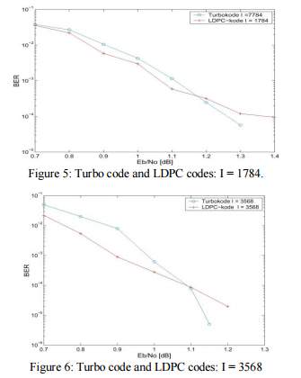
A brief comparison of Turbo codes and LDPC codes are given during this section, each in term of performance and quality. so as to present a good comparison of the codes, we have a tendency to use codes of constant input word length once examination. The speed of each codes is R = 1/2. Figures five and six show the performance of Turbo codes and therefore the LDPC codes with info length 1784 and 3568 severally.
The Turbo codes outlined in six were used for getting the performance curves. For each code lengths the LDPC codes square measure higher till a precise S/N is reached, severally Eb/N0 = 1.15 and 1.1 dB. This characteristic ’error floor’ or ’knee’ was conjointly typical of Turbo codes in earlier years, however this has diminish of a drag latterly as a result of the definition of fine permutation matrices..
In order to check the quality of the codes, the quantity of multiplications, additions and sophisticated operations like log, tanh, e and tanh-1 were counted in each codes. Figure eight shows the quantity of operation per iteration for the LDPC and Turbo codes of length I = 1784 and 3568. the quantity of iterations used might vary within the case of the LDPC codes, because the secret writing quality might simply be checked, i.e. that if a legitimate code word is decoded, the secret writing could also be stopped. Hence, there’ll be less and fewer iterations performed the upper the S/N. Hence, so as to characterize the quality, a representative variety was chosen so as to grant a good comparison with Turbo codes: With the higher than parameters the bit error rate for the LDPC code was zero.0038 and 0.00054 for the I = 1784 and that i = 3568 codes severally, whereas for the Turbo code the bit error rate was zero.0043 and 0.00062 severally, i.e. the error rates were sufficiently similar for a good comparison to be in Figure five and Figure six.
Because of these advantages of LDPC codes over RS code we are going for LDPC codes.
2.4 Applications
In 2003, an irregular repeat accumulate (IRA) style LDPC code beat six turbo codes to become the error correcting code in the new DVB-S2 standard for the satellite transmission of digital television.[9] The DVB-S2 selection committee made decoder complexity estimates for the Turbo Code proposals using a much less efficient serial decoder architecture rather than a parallel decoder architecture.
This forced the Turbo Code proposals to use frame sizes on the order of one half the frame size of the LDPC proposals. In 2008, LDPC beat convolutional turbo codes as the forward error correction (FEC) system for the ITU-T G.hn standard.[10] G.hn chose LDPC codes over turbo codes because of their lower decoding complexity (especially when operating at data rates close to 1.0 Gbit/s) and because the proposed turbo codes exhibited a significant error floor at the desired range of operation. LDPC codes are also used for 10GBase-T Ethernet, which sends data at 10 gigabits per second over twisted-pair cables.
Some OFDM systems add an additional outer error correction that fixes the occasional errors (the “error floor”) that get past the LDPC correction inner code even at low bit error rates. For example: The Reed-Solomon code with LDPC Coded Modulation (RS-LCM) uses a Reed-Solomon outer code.[13] The DVB-S2, the DVB-T2 and the DVB-C2 standards all use a BCH code outer code to mop up residual errors after LDPC decoding.
Chapter 3
SOFTWARE/HARDWARE REQUIREMENTS
3.1 FPGA
A Field Programmable Gate Array is an integrated circuit designed to be configured by a customer or a designer after manufacturing – hence “field-programmable“. The FPGA configuration is generally specified using a hardware description language (HDL), similar to that used for an application-specific integrated circuit (ASIC). (Circuit diagrams were previously used to specify the configuration, as they were for ASICs, but this is increasingly rare.)

A Spartan FPGA from Xilinx
FPGAs contain an array of programmable logic blocks, and a hierarchy of reconfigurable interconnects that allow the blocks to be “wired together”, like many logic gates that can be inter-wired in different configurations. Logic blocks can be configured to perform complex combinational functions, or merely simple logic gates like AND and XOR. In most FPGAs, logic blocks also include memory elements, which may be simple flip-flops or more complete blocks of memory.
Contemporary field-programmable gate arrays (FPGAs) have large resources of logic gates and RAM blocks to implement complex digital computations. As FPGA designs employ very fast I/Os and bidirectional data buses, it becomes a challenge to verify correct timing of valid data within setup time and hold time. Floor planning enables resources allocation within FPGAs to meet these time constraints. FPGAs can be used to implement any logical function that an ASIC could perform. The ability to update the functionality after shipping, partial re-configuration of a portion of the design[2] and the low non-recurring engineering costs relative to an ASIC design (notwithstanding the generally higher unit cost), offer advantages for many applications.[1]
Some FPGAs have analog features in addition to digital functions. The most common analog feature is programmable slew rate on each output pin, allowing the engineer to set low rates on lightly loaded pins that would otherwise ring or couple unacceptably, and to set higher rates on heavily loaded pins on high-speed channels that would otherwise run too slowly. Also common are quartz-crystal oscillators, on-chip resistance-capacitance oscillators, and phase-locked loops with embedded voltage-controlled oscillators used for clock generation and management and for high-speed serializer-deserializer (SERDES) transmit clocks and receiver clock recovery. Fairly common are differential comparators on input pins designed to be connected to differential signaling channels.
A few “mixed signal FPGAs” have integrated peripheral analog-to-digital converters (ADCs) and digital-to-analog converters (DACs) with analog signal conditioning blocks allowing them to operate as a system-on-a-chip.[5] Such devices blur the line between an FPGA, which carries digital ones and zeros on its internal programmable interconnect fabric, and field-programmable analog array (FPAA), which carries analog values on its internal programmable interconnect fabric.
3.2 Architecture of FPGA
3.2.1 Logic blocks
The most common FPGA architecture consists of an array of logic blocks (called configurable logic block, CLB, or logic array block, LAB, depending on vendor), I/O pads, and routing channels. Generally, all the routing channels have the same width (number of wires). Multiple I/O pads may fit into the height of one row or the width of one column in the array.
An application circuit must be mapped into an FPGA with adequate resources.
While the number of CLBs/LABs and I/Os required is easily determined from the design, the number of routing tracks needed may vary considerably even among designs with the same amount of logic. For example, a crossbar switch requires much more routing than a systolic array with the same gate count. Since unused routing tracks increase the cost (and decrease the performance) of the part without providing any benefit, FPGA manufacturers try to provide just enough tracks so that most designs that will fit in terms of lookup tables (LUTs) and I/Os can be routed. This is determined by estimates such as those derived from Rent’s rule or by experiments with existing designs.
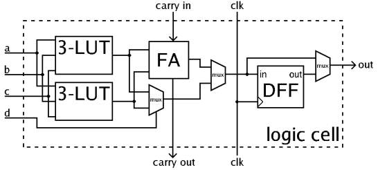
In general, a logic block (CLB or LAB) consists of a few logical cells (called ALM, LE, slice etc.). A typical cell consists of a 4-input LUT, a full adder (FA) and a D-type flip-flop, as shown below. The LUTs are in this figure split into two 3-input LUTs. In normal mode those are combined into a 4-input LUT through the left mux. In arithmetic mode, their outputs are fed to the FA. The selection of mode is programmed into the middle multiplexer. The output can be either synchronous or asynchronous, depending on the programming of the mux to the right, in the figure example. In practice, entire or parts of the FA are put as functions into the LUTs in order to save space.
3.2.2 Hard blocks
Modern FPGA families expand upon the on top of capabilities to incorporate higher level practicality fastened into the semiconductor. Having these common functions embedded into the semiconductor reduces the world needed and offers those functions augmented speed compared to assembling them from primitives. samples of these embrace multipliers, generic DSP blocks, embedded processors, high speed I/O logic and embedded reminiscences. Higher-end FPGAs will contain high speed multi-gigabit transceivers and onerous scientific discipline cores like processor cores, LAN MACs, PCI/PCI specific controllers, and external memory controllers. These cores exist aboard the programmable material, however they’re designed out of transistors rather than LUTs in order that they have ASIC level performance and power consumption whereas not intense a major quantity of material resources, going away a lot of of the material free for the application-specific logic.
The multi-gigabit transceivers conjointly contain high performance analog input and output electronic equipment together with high-speed serializers and deserializers, parts that can’t be designed out of LUTs. Higher-level PHY layer practicality like line coding may or may not be implemented alongside the serializers and deserializers in hard logic, depending on the FPGA.
3.2.3 Clocking
Most of the circuitry built inside of an FPGA is synchronous circuitry that requires a clock signal. FPGAs contain dedicated global and regional routing networks for clock and reset so they can be delivered with minimal skew. Complex designs can use multiple clocks with different frequency and phase relationships, each forming separate clock domains. These clock signals can be generated locally by an oscillator or they can be recovered from a high speed serial data stream. Care must be taken when building clock domain crossing circuitry to avoid metastability. FPGAs generally contain block RAMs that are capable of working as dual port RAMs with different clocks, aiding in the construction of building FIFOs and dual port buffers that connect differing clock domains.
3.2.4 3D architectures
To shrink the scale and power consumption of FPGAs, vendors like Tabula and Xilinx have introduced new 3D or stacked architectures. Following the introduction of its twenty eight nm 7-series FPGAs, Xilinx unconcealed that many of the highest-density components in those FPGA product lines are going to be created victimisation multiple dies in one package, using technology developed for 3D construction and stacked-die assemblies. Xilinx’s approach stacks many (three or four) active FPGA die side-by-side on a element one piece of element that carries passive interconnect. The multi-die construction additionally permits totally different|completely different} components of the FPGA to be created with different method technologies, because the method needs ar totally different between the FPGA material itself and also the terribly high speed twenty eight Gbit/s serial transceivers. associate degree FPGA in-built this manner is named a heterogeneous FPGA. Altera’s heterogeneous approach involves employing a single monolithic FPGA die and connecting alternative die/technologies to the FPGA victimisation Intel’s embedded multi-die interconnect bridge (EMIB) technology.
3.3 Xilinx
Xilinx ISE (Integrated Synthesis Environment) is a software tool produced by Xilinx for synthesis and analysis of HDL designs, enabling the developer to synthesize (“compile”) their designs, perform timing analysis, examine RTL diagrams, simulate a design’s reaction to different stimuli, and configure the target device with the programmer.
Xilinx ISE is a design environment for FPGA products from Xilinx, and is tightly-coupled to the architecture of such chips, and cannot be used with FPGA products from other vendors.[3] The Xilinx ISE is primarily used for circuit synthesis and design, while ISIM or the Model Sim logic simulator is used for system-level testing. Other components shipped with the Xilinx ISE include the Embedded Development Kit (EDK), a Software Development Kit (SDK) and Chip Scope Pro.
Since 2012, Xilinx ISE has been discontinued in favor of Vivado Design Suite, that serves the same roles as ISE with additional features for system on a chip development.[7] Xilinx released the last version of ISE in October 2013(version 14.7), and states that “ISE has moved into the sustaining phase of its product life cycle, and there are no more planned ISE releases.
3.4 Optical Transmission System
Fiber-optic communication could be a methodology of transmittal info from one place associate degree other to a different by causing pulses of sunshine through a glass fiber. The sunshine forms associate magnetic force carrier that’s modulated to hold info. Fiber is most well-liked over electrical cabling once high information measure, long distance, or immunity to magnetic force interference are needed.
Optical fiber is employed by several telecommunications corporations to transmit phone signals, web communication, and cable tv signals. Researchers at Bell Labs have reached internet speeds of over 100 petabit×kilometer per second using fiber-optic communication.
Advantages
Short distance and comparatively low information measure applications, electrical transmission is usually most well-liked due to its
- Lower material value, wherever massive quantities aren’t needed
- Lower value of transmitters and receivers
- Capability to hold electrical power as well as signals (in appropriately designed cables).
- Ease of operating transducers in linear mode.
- Crosstalk from nearby cables and other parasitical unwanted signals increase profits from replacement and mitigation devices.
Optical fibers are more difficult and expensive to splice than electrical conductors. And at higher powers, optical fibers are susceptible to fiber fuse, resulting in catastrophic destruction of the fiber core and damage to transmission components.[23]
Because of these benefits of electrical transmission, optical communication is not common in short box-to-box, backplane, or chip-to-chip applications; however, optical systems on those scales have been demonstrated in the laboratory.
In certain situations fiber may be used even for short distance or low bandwidth applications, due to other important features:
- Immunity to electromagnetic interference, including nuclear electromagnetic pulses.
- High electrical resistance, making it safe to use near high-voltage equipment or between areas with different earth potentials.
- Lighter weight important, for example, in aircraft.
- No sparks, important in flammable or explosive gas environments.
- Not electromagnetically radiating, and difficult to tap without disrupting the signal, important in high-security environments.
- Much smaller cable size, important where pathway is limited, such as networking an existing building, where smaller channels can be drilled and space can be saved in existing cable ducts and trays.
- Resistance to corrosion due to non-metallic transmission medium.
3.5 Verilog
Verilog high-density lipoprotein is one in every of the two common Hardware Description Languages (HDL) employed by integrated circuit (IC) designers. the opposite one is VHDL. HDL’s permits style|the planning|the look} to be simulated earlier within the design cycle so as to correct errors or experiment with completely different architectures. styles represented in high-density lipoprotein ar technology-independent, simple to style and correct, and ar sometimes additional legible than schematics, significantly for giant circuits.
Verilog is accustomed describe styles at four levels of abstraction:
Algorithmic level (much like c code with if, case and loop statements).
Register transfer level (RTL uses registers connected by mathematician equations).
Gate level (interconnected AND, NOR etc)
Switch level (the switches area unit MOS transistors within gates).
The language conjointly defines constructs that may be wont to management the input and output of simulation. additional recently Verilog is employed as AN input for synthesis programs which can generate a gate-level description (a netlist) for the circuit. Some Verilog constructs aren’t synthesizable. Cojointly the approach the code is written can greatly impact the scale and speed of the synthesized circuit.
Most readers can wish to synthesize their circuits, therefore non synthesizable constructs ought to be used just for check benches. These area unit program modules wont to generate I/O required to simulate the remainder of the planning. The words “not synthesizable” are going to be used for examples and constructs PRN that don’t synthesize.
There area unit 2 sorts of code in most HDLs: Structural, that could be a verbal schematic while not storage.
assign a=b & c | d; /* “|” could be a OR */
assign d = e & (~c);
Gate level (interconnected AND, NOR etc.).
Here the order of the statements doesn’t matter. dynamic e can amendment a.
Procedural that is employed for circuits with storage, or as a convenient thanks to write conditional logic.
always @(posedge clk) // Execute following statement on each rising clock edge.
count <= count+1;
Procedural code is written like c code and assumes each assignment is hold on in memory till over written. For synthesis, with flip-flop storage, this kind of thinking generates an excessive amount of storage. but folks like procedural code as a result of it’s typically a lot of easier to put in writing, as an example, if and case statements area unit solely allowed in procedural code. As a result, the synthesizers are created which may acknowledge bound varieties of procedural code as really combinative.
Chapter 4
INTRODUCTION TO LDPC CODES
4.1 LDPC CODES:
In information theory, a low-density parity-check (LDPC) code is a linear error correcting code, a method of transmitting a message over a noisy transmission channel. An LDPC is constructed using sparse bipartite graph.[3] LDPC codes are capacity-approaching codes, which means that practical constructions exist that allow the noise threshold to be set very close (or even arbitrarily close on the BEC) to the theoretical maximum (the Shannon limit) for a symmetric memory less channel. The noise threshold defines an upper bound for the channel noise, up to which the probability of lost information can be made as small as desired. Using iterative belief propagation techniques, LDPC codes can be decoded in time linear to their block length.
LDPC codes are finding increasing use in applications requiring reliable and highly efficient information transfer over bandwidth or return channel-constrained links in the presence of corrupting noise. Implementation of LDPC codes has lagged behind that of other codes, notably turbo codes.
Low-density parity-check (LDPC) codes are forward error-correction codes, first proposed in the 1962 PhD thesis of Gallager at MIT. At the time, their incredible potential remained undiscovered due to the computational demands of simulation in an era when vacumm tubes were only just being replaced by the first transistors. They remained largely neglected for over 35 years. In the mean time the field of forward error correction was dominated by highly structured algebraic block and convolutional codes. Despite the enormous practical success of these codes, their performance fell well short of the theoretically achievable limits set down by Shannon in his seminal 1948 paper. By the late 1980s, despite decades of attempts, researchers were largely resigned to this seemingly insurmountable theory practice gap.
The relative quiescence of the coding field was utterly transformed by the introduction of “turbo codes,” proposed by Berrou, Glavieux and Thitimajshima in 1993, wherein all the key ingredients of successful error correction codes were replaced: turbo codes involve very little algebra, employ iterative, distributed algorithms, focus on average (rather than worst-case) performance, and rely on soft (or probabilistic) information extracted from the channel. Overnight, the gap to the Shannon limit was all but eliminated, using decoders with manageable complexity.
As researchers struggled through the 1990s to understand just why turbo codes worked as well as they did, two researchers, McKay and Neal, introduced a new class of block codes designed to posses many of the features of the new turbo codes. It was soon recognized that these block codes were in fact a rediscovery of the LDPC codes developed years earlier by Gallager. Indeed, the algorithm used to decode turbo codes was subsequently shown to be a special case of the decoding algorithm for LDPC codes presented by Gallager so many years before.
New generalizations of Gallager’s LDPC codes by variety of researchers together with Luby, Mitzenmacher, Shokrollahi, Spielman, Richardson and Urbanke, made new irregular LDPC codes that simply exceed the most effective turbo codes, furthermore as providing sure sensible benefits associated an arguably cleaner setup for theoretical results. Today, style techniques for LDPC codes exist that change the development of codes that approach the Shannon’s capability to inside hundredths of a sound unit.
So rapid progress has been in this area that coding theory today is in many ways unrecognizable from its state just a decade ago. In addition to the strong theoretical interest in LDPC codes, such codes have already been adopted in satellite-based digital video broadcasting and long-haul optical communication standards, are highly likely to be adopted in the IEEE wireless local area network standard, and are under consideration for the long-term evolution of third generation mobile telephony.
4.2 Error correction using parity-checks
Here we will only consider binary messages and so the transmitted messages consist of strings of 0’s and 1’s. The essential idea of forward error control coding is to augment these message bits with deliberately introduced redundancy in the form of extra check bits to produce a codeword for the message. These check bits are added in such a way that code words are sufficiently distinct from one another that the transmitted message can be correctly inferred at the receiver, even when some bits in the codeword are corrupted during transmission over the channel. The simplest possible coding scheme is the single confirmation code (SPC). The SPC involves the addition of one further bit to the binary message, the worth of that depends on the bits within the message. In a fair parity code, the extra bit supplemental to {every} message ensures a fair variety of 1s in every codeword.
Example 1:
The 7-bit American Standard Code for Information Interchange string for the letter S is 1010011, and a bit is to be supplemental because the eighth bit. The string for S already has a fair variety of ones (namely four) so the worth of the bit is zero, and also the codeword for S is 10100110.
SOLUTION
More formally, for the 7-bit American Standard Code for Information Interchange and even parity code we tend to outline a codeword c to possess the subsequent structure:
c = [c1 c2 c3 c4 c5 c6 c7 c8],
where every ci is either zero or one, and each codeword satisfies the constraint
c1 ⊕ c2 ⊕ c3 ⊕ c4 ⊕ c5 ⊕ c6 ⊕ c7 ⊕ c8 = zero. (1.1)
Equation (1.1) is called a parity-check equation, in which the symbol ⊕ represents modulo-2 addition.
While the inversion of a single bit due to channel noise can easily be detected with a single parity check code, this code is not sufficiently powerful to indicate which bit, or indeed bits, were inverted. Moreover, since any even number of bit inversions produces a string satisfying the constraint (1.1), patterns of even numbers of errors go undetected by this simple code. Detecting more than a single bit error calls for increased redundancy in the form of additional parity bits and more sophisticated codes contain multiple parity-check equations and each codeword must satisfy every one of them.
Example 2
A code C consists of all length six strings
c = [c1 c2 c3 c4 c5 c6],
which satisfy all three parity-check equations:
c1 ⊕ c2 ⊕ c4 = 0
c2 ⊕ c3 ⊕ c5 = 0
c1 ⊕ c2 ⊕ c3 ⊕ c6 = 0
Codeword constraints are often written in matrix form and so the constraints of (1.2) become

The matrix H is called a parity-check matrix. Each row of H corresponds to a parity-check equation and each column of H corresponds to a bit in the codeword. Thus for a binary code with m parity-check constraints and length n code words the parity-check matrix is an m × n binary matrix.
In matrix form a string y = [c1 c2 c3 c4 c5 c6] is a valid codeword for the code with parity-check matrix H if and only if it satisfies the matrix equation
Hy T = 0.
4.3 Encoding
To distinguish between the message bits and parity bits in the codeword in Example 1.3 we re-write the code parity-check constraints so that each one solves for a different codeword bit.
Example 1.4.
The code constraints from Example 1.3 can be re-written as
c4 = c1 ⊕ c2
c5 = c2 ⊕ c3
c6 = c1 ⊕ c2 ⊕ c3 (1.5)
The codeword bits c1, c2, and c3 contain the three bit message, c1, c2, and c3, while the codeword bits c4, c5 and c6 contain the three parity-check bits. Written this way the codeword constraints show how to encode the message.
Example 1.5.
Using the constraints in (1.5) the message 110 produces the parity-check bits
c4 = 1 ⊕ 1 = 0,
c5 = 1 ⊕ 0 = 1,
c6 = 1 ⊕ 1 ⊕ 0 = 0,
and so the codeword for this message is c = [1 1 0 0 1 0].
Again these constraints can be written in matrix form as follows:
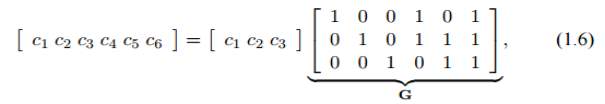
where the matrix G is termed the generator matrix of the code. The message bits square measure conventionally labelled by u = [u1, u2, · · · uk], wherever the vector u holds the k message bits. therefore the codeword c adore the binary message u = [u1u2u3] are often found victimization the matrix equation
c = uG.
For a binary code with k message bits and length n code words the generator matrix, G, is a k × n binary matrix. The ratio k/n is called the rate of the code. A code with k message bits contains 2 k code words. These code words are a subset of the total possible 2 n binary vectors of length n.
Example 1.3:
[0 0 0 0 0 0] [0 0 1 0 1 1] [0 1 0 1 1 1] [0 1 1 1 0 0]
[1 0 0 1 0 1] [1 0 1 1 1 0] [1 1 0 0 1 0] [1 1 1 0 0 1] (1.8)
This code is called systematic because the first k codeword bits contain the message bits. For systematic codes the generator matrix contains the k × k identity, Ik, matrix as its first k columns. (The identity matrix, Ik, is a k × k square binary matrix with ‘1’ entries on the diagonal from the top left corner to the bottom right corner and ‘0’ entries everywhere else.)
A generator matrix for a code with parity-check matrix H can be found by performing Gauss-Jordan elimination on H to obtain it in the form
H = [A, In−k], (1.9)
where A is an (n−k)×k binary matrix and In−k is the identity matrix of order n − k. The generator matrix is then
G = [Ik, AT ]. (1.10)
The row space of G is orthogonal to H. Thus if G is the generator matrix for a code with parity-check matrix H then
GH^T = 0.
Before concluding this section we note that a block code can be described by more than one set of parity-check constraints. A set of constraints is valid for a code provided that equation (1.4) holds for all of the code words in the code. For low-density parity-check codes the choice of parity-check matrix is particularly important.
4.4 Error Detection and Correction
Suppose a codeword has been sent down a binary symmetric channel and one or additional of the codeword bits could are flipped. The task, define during this section and therefore the following, is to notice any flipped bits and, if potential, to correct them. Firstly, we all know that each codeword within the code should satisfy (1.4), so errors is detected in any received word that doesn’t satisfy this equation.
Example 1.8.
The codeword c = [1 0 1 1 1 0] from the code in Example 1.3 was sent through a binary symmetric channel and the the string y = [1 0 1 0 1 0] received. Substitution into equation (1.4) gives
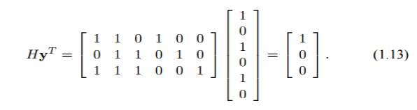
The result is nonzero and so the string y is not a codeword of this code. We therefore conclude that bit flipping errors must have occurred during transmission .The vector
s = Hy^ T ,
is called the syndrome of y. The syndrome indicates which parity-check constraints are not satisfied by y.
Example 1.9.
The result of Equation 1.13, in Example 1.8, (i.e. the syndrome) indicates that the first parity-check equation in H is not satisfied by y. Since this parity-check equation involves the 1-st, 2-nd and 4-th codeword bits we can conclude that at least one of these three bits has been inverted by the channel.
Example 1.8
Demonstrates the use of a block code to detect transmission errors, but suppose that the channel was even noisier and three bits were flipped to produce the string y = [0 0 1 0 1 1]. Substitution into (1.4) tells us that y is a valid codeword and so we cannot detect the transmission errors that have occurred. In general, a block code can only detect a set of bit errors if the errors don’t change one codeword into another.
The Hamming distance between two code words is defined as the number of bit positions in which they differ. For example the code words
[1 0 1 0 0 1 1 0] and [1 0 0 0 0 1 1 1] differ in two positions, the third and eight codeword bits, so the Hamming distance between them is two. The measure of the ability of a code to detect errors is the minimum Hamming distance or just minimum distance of the code. The minimum distance of a code, dmin, is defined as the smallest Hamming distance between any pair of code words in the code. For the code in Example 1.3, dmin = 3, so the corruption of three or more bits in a codeword can result in another valid code word. A code with minimum distance dmin, can always detect t errors whenever
t<dmin (1.14)
To go further and proper the bit flipping errors needs that the decoder confirm that codeword was possibly to possess been sent. based mostly solely on knowing the binary received string, y, the most effective decoder can select the codeword nearest in performing distance to y. once there’s over one codeword at the minimum distance from y the decoder can arbitrarily select one in all them. This decoder is termed the most chance (ML) decoder because it can continually selected the codeword that is possibly to possess made y.
The minimum distance of the code in Example 1.8 is 3, so a single bit flipped always results in a string y closer to the codeword which was sent than any other codeword and thus can always be corrected by the ML decoder. However, if two bits are flipped in y there may be a different codeword which is closer to y than the one which was sent, in which case the decoder will choose an incorrect codeword.
In general, for a code with minimum distance dmin, e bit flips can always be corrected by choosing the closest codeword whenever
e≤⌊(dmin−1)/2⌋, (1.15)
where ⌊x⌋ is the largest integer that is at most x. The smaller the code rate the smaller the subset of 2 n binary vectors which are code words and so the better the minimum distance that can be achieved by a code with length n. The importance of the code minimum distance in determining its performance is reflected in the description of block codes by the three parameters (n, k, dmin).
Error correction by directly comparing the received string to every other code word in the code, and choosing the closest, is called maximum likelihood decoding because it is guaranteed to return the most likely codeword. However, such an exhaustive search is feasible only when k is small. For codes with thousands of message bits in a codeword it becomes far too computationally expensive to directly compare the received string with every one of the 2 k code words in the code. Numerous ingenious solutions have been proposed to make this task less complex, including choosing algebraic codes and exploiting their structure to speed up the decoding or, as for LDPC codes, devising decoding methods which are not ML but which can perform very well with a much reduced complexity.
4.5 Design Approach
Clearly, the most obvious path to the construction of an LDPC code is via the construction of a low density parity check matrix with prescribed properties. A large number of design techniques exist in the literature, and we introduce some of the most prominent ones in this section, albeit at the superficial level. The design approaches target different design criteria , including efficient encoding and decoding , near capacity performance or low error rate floors(Like Turbo Codes ,LDPC codes often suffer from low error rate floors, owing to both poor distance spectra and weakness in the iterative decoding algorithm).
4.5.1 Gallager Codes
The original Ldpc codes due to gallager [1] are regular ldpc codes with a H-matrix of the form
Where the submatrices Hd have the following structure . Further such codes have low complexity encoders since parity bits can be solved foras a function of the user bits via the parity check matrix . Gallager codes were generalised by Tanner in 1981 and were studied for an application to code division multiple access communication channel. Gallager codes were extended by Mac Kay and others[3],[4].
4.5.2 MacKay Codes
Mackay had independently discovered the benefits of desigining binary codes with sparse H matrices and was the first to show the ability of these codes to perform near capacity limits[3],[4].Mackay has archived on a web page [10] a large number of ldpc codes he has deigined for application to data communication and storage ,most of which are regular. He provided in[4] algorithms to semi-randomly generate sparse H matrices. One drawback of Mackay codes is that they lack sufficient structure to enable low complexity encoding .
4.5.3 RA, IRA And eIRA codes
A type of code, called a repeat-accumulate(RA) code, which has the characteritics of both serial turbo codes and LDPC codes, was proposed in 1920 . The encoder for an RA code is shown in fig where it is seen that user bits are repeated (2 or 3 times typical), permuted, and then sent through an accumulater(differentia encoder). These codes have been shown to be capable of operation near capacity limits, but they have the drawback that thet are naturally low rate( rate 1/2 or lower).
The RA codes were generalised n such a way that some bits were repeated more than others yielding irregular repeat accumulate(IRA codes). As shown in figure, the IRA encoder comprises a low density generator matrix, a permuter and an accumuator. Such codes are capable of operation even closer to theoritical limits than RA codes, and they permit higher code rates. A drawback to IRA codes is that they are nominally non systemically. Although they be put in systematic form. But it is at the expense of greatly lowering the rate as depicated in figure.
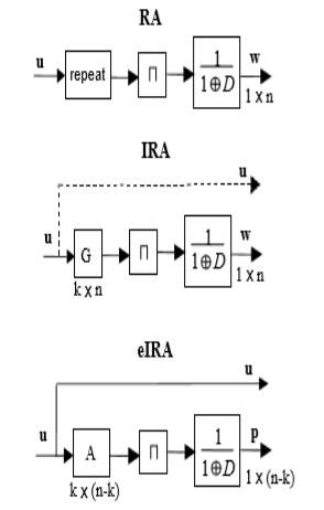
Yang and ryan have proposed a class of efficiently encodable irregular LDPC codes which might be called extented IRA codes( these codes where independently proposed). The eIRA encoder is shown in figure. Note that the eIRA encoder is systematic and permits both low and high rates. Future encoding can be efficiently performed directly from the H matrix which possesses and m*n sub matrix which facilitates computation of the parity bits from the user bits.
4.6 STATE-OF-THE-ART FEC CODES FOR NEXT GENERATION OPTICAL NETWORKS
In current and next generation optical communications very powerful FEC codes are essential to enhance the transmission reach. A minimum post-FEC BER of 10^−12 or preferably 10^−15 is generally required. Currently, the most popular schemes for FEC codes targeting 100G systems are based on Turbo, LDPC and interleaved-concatenated coding concepts. We note that the construction of FEC codes has been a highly active research area for a very long time and therefore we will describe only the most recent and efficient codes available in the open literature. Information about the status of commercialization, patented solutions and the relative academic research is provided as well.
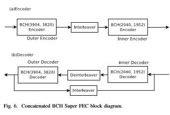
4.6.1 Two-iteration Concatenated BCH code:
The described concatenated BCH code [23] consists of an outer BCH (3904,3820) and an inner BCH(2040,1952), and has approximately 6.81% redundancy. On this decoder low-complexity syndrome computation architecture and a high-speed dual-processing pipelined simplified Berlekamp-Massey key equation solver architecture is applied. High throughput, low complexity and high correction ability are achieved with the use of block interleaving methods and the development of the two-parallel processing method by converting the frame format. The two-parallel architecture needs the frame converter in order to parallelize two serial frames at input and output port of the two-iteration concatenated BCH decoder.
Additionally, in order to keep the hardware complexity low the number of iterations was selected to be two, since the two-iteration scheme requires a lower number of inner and outer decoders as well as interleavers/deinterleavers than the three-iteration scheme. Figure 6 depicts a block diagram of the described two-iteration concatenated. From post-layout simulation, the achieved NCG is 8.91d Bat an output BER of 10^−15 and the latency is 11.8 µs. The maximum clock frequency at which this architecture can operate is 430MHz in 90nm CMOS technology and the data processing rate is 110 Gb/s.
The total variety of gates and space usage for the planned two-iteration concatenated BCH decoder area unit 1,928,000 and interleavers/deinterleavers, frame converters and FIFOs. the desired memory size for the two-iteration concatenated BCH decoder is just about 155kbytes as well as all FIFOs, two frame converters, one interleaver and a couple of deinterleavers.
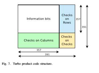
4.6.2 Turbo Product Code with shortened BCH component codes:
The HD-based ”Turbo Product Code” scheme, proposed in [24], has an overhead of 20% as recommended by OIF (Optical Internetworking Forum) and achieves 10dB NCG after 8 iterations. Its structure is shown in Figure 7. For its construction, shortened BCH (391, 357) component codes in GF(211) are used. In each BCH component code, the first 1656 bits are fixed to 0’s, the middle 357 bits are information bits and the last 34 bits are parity check bits. The product code is then shortened by removing all fixed 0’s and this returns a product code with shortened BCH component codes. For the decoding, each shortened component code aims to correct up to 3 errors. During one iteration both rows and columns are decoded once. The standard procedure for the component code decoding algorithm consists of three steps:
• restore the BCH code,
• decode BCH code, and
• use the shortened bits for further checks.
As regards its hardware implementation, the algorithm used for the decoding of the individual BCH codes takes advantage of the property that the shift of a BCH codeword is also a codeword. Therefore, for a codeword of length n, n rounds are required to get the decoding result.
4.6.3 LDPC-Based Codes:
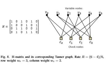
In coding theory, a parity-check matrix of a linear block code C is a matrix which describes the linear relations that the components of a codeword must satisfy. If the parity check matrix has a low density of 1’s and the number of 1’s per column (wc: column weight) and per row (wr: row weight) are both constant, the code is said to be a regular Low-Density Parity-Check (LDPC) code. If the parity-check matrix has low density, but the number of 1’s per row or column varies, the code is said to be an irregular LDPC code. The code rate R is given by the following equation:
R = (n−m)/n = 1−wc/wr.
The graphical representation of LDPC codes, known as bipartite (Tanner) graph representation, is helpful in efficient description of LDPC decoding algorithms (Figure 8). A bipartite (Tanner) graph is a graph whose nodes may be separated into two classes (variable and check nodes), and where undirected edges may only connect two nodes not residing in the same class. The Tanner graph of a code is drawn according to the following rule: check (function) node c is connected to variable node u whenever element hcu in a parity check matrix H is an 1. In an m × n parity-check matrix, there are m = n−k check nodes and n variable nodes. A closed path in a bipartite graph compromising l edges that closes back on itself is called a cycle of length l. The shortest cycle in the bipartite graph is called the girth.
The girth influences the minimum distance of LDPC codes, correlates the extrinsic log-likelihood ratios (LLRs) and, therefore, affects the decoding performance. Hence, the use of large girth LDPC codes is generally preferable. The iterative schemes used for their decoding engage passing the extrinsic information back and forth among the check and the variable nodes over the edges to update the distribution estimation. Conventionally, the sum-product algorithm (SPA) [25] or the modified min sum algorithm (MSA) [26] is used. However, layered LDPC decoding schemes have recently attracted much attention in both academy and industry because they can effectively speed up the convergence of LDPC decoding and thus reduce the required maximum number of decoding iterations. At present, two kinds of layered decoding approaches have been proposed:
- row-layered decoding [27]–[30] and
- column-layered decoding [30]–[32].
In row-layered decoding, the rows of the parity check matrix are grouped into layers and the message updating is performed row layer by row layer, whereas in column layered decoding this matrix is partitioned into column layers and the update happens column layer by column layer.
LDPC codes and especially Quasi-Cyclic LDPCs (QCLDPC) seem to be strong candidates for SD-FEC codes in next generation optical networks, due to their efficient parallelization and low complexity (required for 100G and beyond optical communication). Despite their advantages, these codes have a major drawback, which is the appearance of error floor. Thus various approaches have been proposed for the elimination of this phenomenon. Figure 9 depicts three different ways (no code concatenation, regular concatenation, triple concatenation) of using LDPC codes for the construction of FEC frames suitable for 100 Gb/s digital coherent systems, with a 20% overhead, as recommended by the OIF.
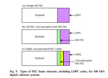
Figure 9a shows a single 20% LDPC implementation. In that case, while a good performance is expected, the effort to eliminate the error floor usually leads to very long code words, resulting in large circuits with high latency. Especially for implementations according to the OTU4 framer, huge interconnection speed between the OTU4 framer LSI and the coherent ASIC is required [33].
Recently, D. Chang et al. [34] and D. A. Morero et al. [35], [36] have made significant progress in the development of efficient single/non-concatenated LDPC codes with low error floor and tolerable latency. In more detail, Huawei’s D. Chang et al. proposed in 2011 a non concatenated girth-8 QC-LDPC(18360, 15300) code exceeding a net coding gain up to 11.3dB, Q-limit of 5.9dB and no error floor at a post-FEC BER of 10^−15. Influenced by the compromise of performance and complexity, wc = 4 (column weight) and wr = 24 (row weight) were selected. Moreover, progressive edge growth (PEG) algorithm was used for the search of high girth QC-LDPC codes. Thanks to the use of modified offset min-sum decoding algorithm with multi thresholds and modified layered decoding algorithm with 4 quantization bits the implementation complexity was kept low [34].
Additionally, D. A. Morero et al. presented a non concatenated QC-LDPC code with a standard 20% or better overhead providing a net effective coding gain greater than 10dB at a BER of 10^−15. In [35], [36] a design method of parity check matrices with reduced number of short cycles, a parallel decoder architecture and an adaptive quantization post-processing technique are described.
Besides these codes, large girth block-circulant LDPCs with 20% redundancy were presented in [37], providing a net effective coding gain of 10.95dB at post-FEC BER of 10^−12, whereas Q. Yang et al. showed in [38] an error free beyond 1 Tb/s QC-LDPC coded 16-QAM CO-OFDM transmission over 1040km standard single-mode fiber and proved its better performance compared to common 4-QAM transmission. However, the routing congestion problem and the increase of the global wiring overhead (due to the feedback-loop architecture of an LDPC block code (LDPC-BC) decoder) should still be considered for the implementation of such long codes (both of them limit the clock frequency and require larger space and power consumption than the initial estimation).
Nevertheless, these two implementation drawbacks can be over comed with the use of LDPC convolutional codes (LDPC-CCs). As can be seen in [39], the LDPC-CCs are suitable for pipelined implementation and additionally their coding performance is similar to this of longer LDPC-BCs. To be more specific, the LDPC-CC(10032,4,24) achieves a Q-factor of 5.7dB and a NCG of 11.5db at a post-FEC BER of 10^−15, as proved by FPGA (Field-Programmable Gate Array) emulation (the maximum number of iterations was set to 12).
Figure 9b presents another way to suppress the unwanted error floor by concatenating a SD-FEC with a HD code. In their paper [40], T. Mizuochi et al. presented the concatenation of LDPC (9216,7936) and RS(992,956) codes, achieving a NCG of 9db at 10^−13 with only 2-bit soft-decision and 4 iterations. In order to guarantee low circuit complexity and high error correction performance, cyclic approximated δ-minimum algorithm is proposed for the decoding procedure. The value of row and column weight is 36 and 5, respectively, whereas the girth of the LDPC code is 6. Under this concept, another high-performance low-complexity approach based on LDPC codes are the ”Concatenated QC-LDPC and SPC Codes“, introduced by N. Kamiya and S. Shioiri (NEC Corporation) [41].
The construction of these codes rely on the concatenation of single-parity check (SPC) codes and QC-LDPC codes of shorter lengths. According to the OTU4 framer, an implementation with 20.5% OH is proposed. The expected Q-limit and NCG of these codes, with 4 quantized bits and 15 iterations are 5.8 dB and 10.4 dB at a BER of 10^−12( NCG=11.3 dB at a BER of 10^−15), respectively. Naturally, a small degradation in the performance is noticed with the reduction in the number of quantization levels or in the maximum number of iterations. ”Spatially-coupled codes“ is another class of LDPCs, which can be derived from QC-LDPC design [42].
Numerical simulation (Monte Carlo simulation in an additive white Gaussian noise channel with QPSK modulation) [43] indicate a NCG of 12.0 dB at a BER of 10^−15 achieved by the code concatenation of spatially coupled type irregular LDPC(38400, 30832) and BCH(30832, 30592), when the number of iterations was set to 32. This scheme has a 25.5% redundancy and for its decoding the simplified δ-min algorithm with 4 soft-decision bits was used. Another promising FEC scheme for100Gb/s Optical Transport Systems is the recently presented ”Concatenated Non-Binary LDPC and HD-FEC Code“ [44].
The proposed concatenated NB-LDPC(2304,2048) over GF(24) and RS(255,239) is compatible with OTU-4 frame structure and can provide a NCG performance over 10.3 dB at a post-FEC BER 10^−15 and over 10.8 dB with enhanced HD-FEC in the outer code, with the number of maximum iteration limited to 16. As far as its architecture modeling is concerned, between NB-LDPC and RS codes 2D-interleaving/deinterleaving buffers are located and Min-Max algorithm is preferred for decoding due to its advantageous VLSI implementation compared to FFT-BP algorithms.
Figure 9c illustrates the concept of the so-called ”triple concatenated FEC“ [45]–[48]. Unlike conventional concatenated codes, the proposed one combines an inner LDPC code with a pair of concatenated hard decision based block codes having 7% redundancy.
The expected net coding gain at a 10−15 output BER is 10.8 dB. Generally, these codes are characterized by the following:
• Inner Codes: Irregular QC-LDPC(4608,4080)
• 20.5% total redundancy compliant with OIF standards, which results in a transmission rate of 127.156 Gb/s.
• an OTU4V frame format compliant with ITU-T G.709.
• Decoding algorithm: Variable Offset Belief Propagation
• 16 iterations
• straightforward circuit implementation via a well designed parallelized pipelined architecture.
Recently, non binary approaches are also attracting more and more attention. These codes are designed over higher order fields and achieve coding gains similar to or even better than binary LDPC codes, but for shorter codeword lengths [49], [50]. The higher performance of Non binary LDPC (NBLDPC) codes in comparison to binary ones was at first demonstrated by Davey and Mackay in [51] and [52]. The main factors that led to improved performance are the reduced probability of forming short cycles when compared to their binary counterparts and the increased number of non binary check and variable nodes, which ultimately improves the achievable decoding performance. Their main drawback though, is that they are characterized by increased decoding complexity, due to the large number of values [53].
For the construction of NBQC-LDPC codes firstly finite fields are used for the generation of a large girth parity-check matrix for binary QC-LDPC and then with the application of certain design criteria non zero elements from the Galois field GF(q) replace the ”1“s. With the use of these codes (20% overhead) a net effective coding gain of 10.8 dB at a post-FEC BER of 10−^12 can be achieved [49]. Furthermore, in most recent publications, e.g. [54], NB-QC-LDPC based coded modulation schemes are presented.
Compared to binary interleaved LDPC based coded modulation, the non-binary scheme provides higher coding gains and is advantageous due to the reduced system’s complexity and latency.
In more detail, non binary LDPC coded modulation provides several advantages compared to binary counterparts, when decoding is based on modified FFT based q-ary SPA (MD-FFT-QSPA), as shown in [55]. Namely, with MD-FFT-QSPA, the trade-off between the computational complexity and coding gain improvement can be adjusted to suit the needs of the system under consideration. This particular scheme is also suitable for rate adaptation.
4.6.4 Staircase Codes:
B. P. Smith et al. presented in their paper “Staircase Codes: FEC for 100 Gb/s OTN” [56] a new class of high-rate binary error correcting codes, whose construction combines ideas from recursive convolutional and block coding. These codes are characterized by the relationship between successive matrices of symbols and can be interpreted as generalized LDPC codes with a systematic encoder and an indeterminate block length, which admits decoding algorithms with a range of latencies.
The low latency of their encoding process is guaranteed by the use of a frame mapper, whereas a range of strategies with varying latencies can be used for their decoding due to the fact that these codes are naturally unterminated(i.e. their block length is indeterminate). That is, their decoding can be accomplished in a sliding-window fashion, in which the decoder operates on the received bits (binary case) corresponding to L consecutively received blocks Bi,Bi+1….Bi+L, (Bi denotes an m-by-m matrix with elements either in GF(2) (binary case) or in Galois fields of higher orders (non-binary case)). A more detailed explanation of the encoding and decoding of these codes is provided in [56].
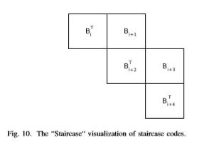
Generally, the relationship between successive blocks in a staircase code satisfies the following relation: for any i >= 1, each of the rows of the matrix [BT i−1,Bi] is a valid codeword. Figure 10 represents a “Staircase” visualization of staircase codes, in which the concatenation of the symbols in every row and every column in the staircase is a valid codeword. The expected NCG from the proposed ITU-T G.709compatible staircase code, with rate R = 239/255 is 9.41dB at an output error rate of 10−15 as evidenced by a FPGA-based simulation.
4.6.5 Multidimensional TPCS and GLPDC Codes with Components RS Codes:
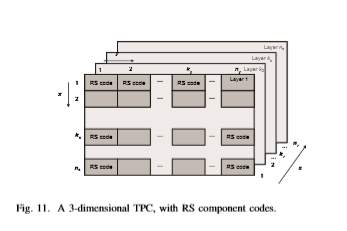
In “Multidimensional Turbo Product and Generalized LDPC Codes with Component RS Codes Suitable for use in Beyond 100 Gb/s Optical Transmission“ paper [57], two hard decision decoding FECs suitable for next generation optical networks are presented. The first scheme is based on multidimensional turbo product codes (MTPCs) with component Reed-Solomon (RS) codes and the second one is based on generalized low-density parity-check (GLDPC) codes with component RS or MTPC codes.
The multidimensional turbo-product codes (MTPCs) are a generalization of the original turbo-product codes. The various methods to perform their encoding and decoding are divided in the following three categories:
• serial,
• fully parallel, and
• partly parallel
In serial version, solely 3 completely different encoders/decoders square measure required, every acting encoding/decoding in corresponding dimension. The encoding/decoding latency of this theme is high, however the quality is low. In totally parallel implementation, we’d like Empire State × nz encoders/decoders acting the encoding/decoding in x-direction, nx ×nz encoders/decoders acting the encoding/decoding in y-direction and nx×ny encoders/decoders acting the encoding/decoding in zdirection. The encoding/decoding latency of this theme is low, whereas the encoding/decoding quality is high.
Thus, the partially parallel scheme was finally proposed for implementation, as a middle ground solution between these two schemes. The three-dimensional (3D)-TPC of rate 0.8, based on (255,237) RS code as a component code, provides the net effective coding gain of 9.3 dB at BER of 10−15 and is also very efficient in dealing burst of errors due to intra-channel nonlinearities.
The GLDPC codes are either constructed using MTPC or RS components for less complex designs. The parity-check matrix H of a Boutros-like non binary GLDPC codes can be partitioned into W sub-matrices H1,…,HW (Eq.1). H1 is a block-diagonal matrix generated from an identity matrix by replacing the ones by the parity-check matrices HMTPC i of the constituent MTPCs of codeword-length N and dimension Ki, i=1,2,…,Nt/N (Eq.2). Nt denotes the code word length of
the GLDPC code. Each sub-matrix Hj is derived from H1 by random permutations πj−1 as given by Eq.3
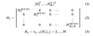
The GLDPC code of rate 0.82, based on (255,239) and (255,223) RS codes as components provides the net effective coding gain of 9.6 dB at BER of 10^−15. Interested readers can find more information about how these schemes are implemented and can be used along with multilevel modulation formats in [57].
4.6.6. Super-Product BCH:
The super-product BCH (SP-BCH) code [58] is a true product code designed for OTU4 100 G applications and was originally introduced by Broadcom Corporation. It has a standard 7% overhead and is based on hard decision decoding. The code consists of 960 BCH(987,956, t=3) (1-bit extended) codes as row codes and 987 BCH(992, 960, t=3) (2-bit extended) codes as column codes. The most likely dead pattern is the 4×4 square error pattern shown in Fig. 12, where 16 bit errors are located in the cross points between 4 arbitrary row codes and 4 arbitrary columns codes.
A maximum number of 7 iterations are allowed at the decoding procedure. Due to an advanced decoding method used for its decoding, called “dynamic reverting”, it is expected to provide a net coding gain up to 9.4 dB for an output BER of 10^−15. The proposed code seems to have advantages, such as lower computational complexity, better burst error correction capacity and less required maximum iterations compared to other super FEC schemes [20]. However, its main drawback is that it has a long decoding latency due to large block size.
Chapter 5
ARCHITECTURE AND IMPLEMENTATION
In this Section, we first provide the overall architecture of our FPGA emulation platform. After that we provide the details of the proposed FPGA architecture for the proposed RC LDPC decoder. The puncturing-based LDPC decoder is used as a reference.
5.1 Overview Of Architecture
The performance of the planned rate adaptive LDPC codes is incontestable employing a set of FPGAs, whose high-level diagram is given in Fig. 1. This high level verification tool is comparable to others according within the literature [6-7] and consists of 3 main parts: a collection of mathematician noise generators, a partly pipelined LDPC decoder, and a slip counter block. The mathematician noise generator generates noise samples employing a combination of Box-Muller algorithmic rule and central limit theorem following the rules in [19]. Such generated sequence of noise samples is increased with variance of noise and fed to the LDPC decoder with measure LLRs.
There are 3 styles of package reconfigurable registers to be initialized within the high-level diagram. the primary set of registers are instantiated to outline the noise variance and also the codeword to be transmitted, the second set of registers to piece the speed adaptive LDPC decoder, together with the amount of superimposed iterations, the number of bit to be cut, and also the variety of generalized check nodes; and also the third set of registers stores the amount of uncoded errors, coded errors, and transmitted.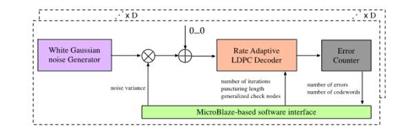 High level schematic of FPGA based evaluation platform
5.2 Rate-Compatible LDPC Decoder Architecture
Figure presents the overview of the reconfigurable binary LDPC decoder, which consists of two parts; namely, memories and processors. The processors can be classified into following categories:
- variable-node processor (VNP) corresponding to Eqn. (5)
- scaled min-sum check-node processor(SMS-CNP) corresponding to Eqn.(7).
- MAP based CNP (MAP-CNP, also referred as generalized CNP) corresponding to Eqn. (6), and
- early termination unit (ETU) corresponding to Eqn. (4).
Four sets of block RAMs are used in the implementation of RC LDPC decoder:
- block RAM with size of × ℎ, stores the channel LLRs,
- block RAM with size of × × stores the messages from check-nodes to variable-nodes,
- block RAM with size of stores the decoded bits, and (iv) additional block RAM inside each CNP stores the intermediate values. In discussion above, denotes the column weight, is the codeword length, and ℎ, represents the bit width for and ℎ,, respectively.
There are two types of reconfigurable routers used in the implementation as well: (i) puncturing-mux is used to select the input either be the outputs of VNP or the largest positive LLR, and (ii) generalized-mux selects either the outputs of SMS-CNP or MAP-CNP. The architecture of SMS-CNP is implemented based on Eqn. (7), which is illustrated in Fig. 2 (b). We first calculate the absolute value and the sign value of the input. Then we find the first and the second minimum values of the absolute values and trace back to find the position of first minimum via binary search tree (BST).
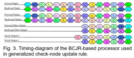
It is worth noting that the number of muxes involved in BST and the latency associated with BST are proportional to the number of inputs. With this technique, we can write back three values and sign bits to the memories instead of values. However, we will not take advantage of memory reduction techniques in the resource utilization comparison study. The implementation of generalized-CNP is based on Eqn. (6), in which MAP function is realized by bidirectional BCJR algorithm. As shown in Fig. 2(c), we first calculate forward- and backward-recursion likelihoods, ( , ) and ( , ), using the input ( ), where , represent the number of states and length of the BCJR trellis that is proportional to the number of check nodes in linear block code and number of the check node degree .
The intermediate values ( ,) and ( ,) are then written into the forward and backward block RAMs. The outputs ( ) are generated by add-max operations, which properly combine forward-likelihood ( ,), backward-likelihood ( ,), and input ( ). The time-variant trellis of a linear block code implies that a precalculated routing scheme should be implemented so that current recursion likelihood can be updated by appropriate previous recursion likelihood.
Furthermore, the max-star-operation is replaced by max-operation due to its high memory consumption as well as additional one cycle needed. The bidirectional recursion scheme is adopted to further reduce the latency of generalized-CNP. For a (15, 11) Hamming code, there are in total of 16 states and the length of trellis is 16 including initial length.
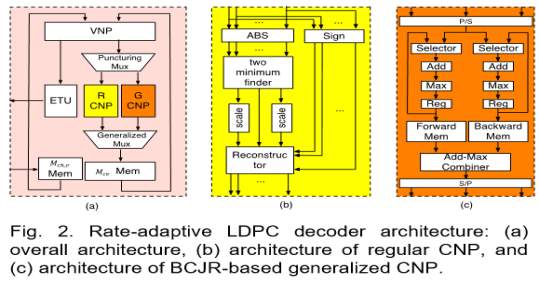
The timing diagram is illustrated in Fig. 3, where ≜ ( ,), ≜ ( ,) represent the forward and backward recursion likelihood vectors of size 16 at time instance . Once half of the forward and backward recursion likelihood have been updated and written into their associate block RAMs, the output 7 is calculated based on current 7 and current 8. Immediately after, two outputs will be generated in each cycle based on current with previous and current with previous .
Thus, the latency of the generalized-CNP can be calculated by = + , + , where , , , represent the latency of parallel-to-serial conversion of the input, length of linear block codes, and the latency of serial-to-parallel conversion of the output.
In summary, the complexity of both SMS-CNP and generalizedCNP are reasonable low, which makes the proposed rate-compatible LDPC code very promising solution for future OTNs.
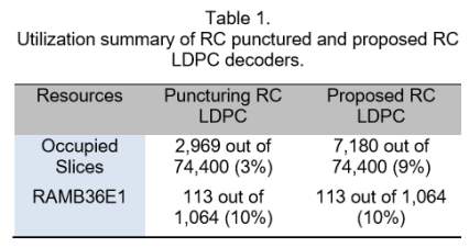
Given the overall architecture described in previous subsection, we implement a (34635, 27710) QC LDPC decoder as well as a generalized version of it using (15, 11) Hamming code, in which there is a set of reconfigurable registers to achieve the rate-adaptive purpose. The utilization reports from Xilinx xc6vsx475t of both punctured LDPC decoder and the proposed RC LDPC decoder are summarized in Table 1.
There are additional 6% in occupied slice usage and 4% in RAMB18E1 usage in the proposed RC LDPC decoder compared to that of the puncturing-based RC LDPC decoder, because the proposed RC LDPC decoder requires one more APP-based CNP to process the data involved in the linear block code.
5.3 Rate-compatible LDPC codes and corresponding decoding algorithms
There exist various algebraic and combinatorial methods to construct structured LDPC codes [12-13]. The large girth QC LDPC code design with column-weight and row-weight based on permutation matrices is adopted due to its low memory usage for storing the paritycheck matrix [13], which can be represented by
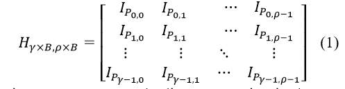
where , represents the × circulant permutation matrix with a location of 1 in row r being at column ( + , ) mod . One straightforward way for rate compatible coding is to design a class of LDPC codes by selecting a class of different code parameters, together with a number of modulations [11]. Later, borrowing the idea from shortening and puncturing of RS codes [14], a puncturing algorithm is proposed that optimizes the degree distribution of a class of LDPC code for a given mother code [15].
Furthermore, rate-adaptive steps LDPC codes show improvement over shortening utilizing a group of interleavers [16]. However, neither of the on top of poses a sufficiently smart hardware structure appropriate for period implementation; in alternative words, no heterogeneous implementation design exists. during this paper, we have a tendency to propose a RC LDPC codes capable of each coarse- and fine-tuning, that allows vital saving on logic and memory recourses.
Given a ( , , ) LDPC code, where , , represent the quantity of variable-nodes, range of knowledge bits, and range of check nodes; the code rate which might be calculated by ≥ 1− / , we are able to scale back the code rate either by reducing or increasing . For coarse-tuning, by setting the initial loglikelihood quantitative relation (LLR) into largest number price, we have a tendency to softly puncture many columns from a mother code that’s diagrammatic by equivalent. (1), whereas we have a tendency to replace many single-parity check (SPC) codes by a linear block code (also referred as generalized codes or native codes) for fine-tuning.
For example, let a QC-LDPC code with = three, = 15, = 1129 be a mother code, puncturing one rightest column in equivalent. (1), the code rate is reduced from zero.8 to 0.7857, that represents the coarse-tuning method. Let denotes the space between 2 neighboring SPC codes to get replaced by an easy linear block code ( , , ), where , , represents the quantity of code bits, range of knowledge bits and range of check bits, severally, once uniform substitution, the code rate will be calculated by ≥ 1− ( +⌊ / ⌋× ( −1))/ .
In step 2, the parity-check matrix is modified either by puncturing several rightmost columns or doping selected SPC codes with simple linear block codes. For completeness of the presentation, we provide the layered decoding algorithm for the proposed RC LDPC codes. Let , , , , and ℎ, represent the check to variable message, the variable to check at -th iteration and -th layer message, and the LLR from the channel, respectively; where = 1,…, and = 1,…, . The layered scaled min-sum algorithm, adopted in this paper, can be summarized as follows [17-18].
Initialization: , = 0 for = 1, = 1,…, (2)
Bit decisions: , = ℎ, +∑ ,′ ′ (3)
̂ = {0, if , ≥ 0 1, otherwise (4)
Variable-node update rule: , = ℎ, +∑ ,′ ′≠ (5)
Check-node update rule:
I. For generalized check-nodes: a posterior probability (APP) update rule is applied:
, = MAP( , ) (6) II. For single-parity check-nodes: scaled min-sum update rule is applied:
, = ×∏ sign( ′ , )min ′≠ | ′ , | ′≠ (7)
where denotes the scaling factor for the minsum algorithm and it is set to 0.75. The above procedure iterates until a pre-defined maximum number of iteration is reached or all decisions are converged to the transmitted codeword, since only 1/ portion of check nodes are involved in each layer.
5.4 Implementation analysis
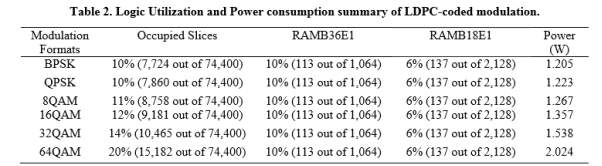
Apart from error correction performance of the rate-adaptive LDPC-coded modulation, logic utilization, power consumption, and latency represent another important aspect. We compare the logic utilization and power consumption of six LDPC-coded modulation schemes, which have been implemented in Xilinx xc6vsx475t. Each emulator comprises 2log ( ) M PRBS generators (M is the signal constellation size), one or two Gaussian noise generator for BPSK and others modulation formats, respectively, one symbol LLR calculator, one bit LLR calculator and one reconfigurable LDPC decoder. The resource utilization is summarized in Table 2.
One can clearly notice that the occupied slices usage increases as the modulation format size increases, while the memory utilization is almost the same due to negligible amount of memory utilization except inside the LDPC decoder.
In addition, the on-chip power consumption from clocks, logics, signals, BRAMs, DSPs, MMCMs, and IOs are shown in the last column in Table 2. The power consumption increases as we increase modulation format size, while this increase is reasonably low.
As we discussed above, we duplicate four LDPC-coded modulation emulators in one FPGA and with four FPGAs available in our rapid prototyping platform, in total 16 emulators are employed. Each decoder consists of 3 CNUs and 45 VNUs in the implementation, hence the throughput of the decoder can be calculated by max /[ /( ) ]clk F n B p I δ × + ×, where 200MHzclkF = is the FPGA running frequency, n is number of bits per codeword, 2309B = is the block size, 3 p = is the pipeline depth, 7 δ = is the latency of VNP and CNP, max 45 I = is the maximum number of layered iterations.
It is worth noting that the decoder will converge fast at high SNR regime (~24 iterations verified by simulation). The aggregation throughput of the mother code will be ~3.17Gbit/s at low SNR regime and ~5.94Gbit/s at high SNR regime, while the throughput of code rate of 0.7 will be ~2.11Gbit/s and ~3.96Gbit/s respectively.
5.5 Proposed rate-adaptive LDPC-coded modulation
The uncoded and coded BER performance vs. SNR of each bit in BPSK, QPSK, 8-QAM, 16QAM, 32-QAM, and 64-QAM are shown in Figs. 3(a) and 3(b), respectively. A close look at Fig. 3 reveals that each bit in higher order modulation is protected unequally. For instance, the first bit and second bit have the same performance (the same applies for the third and the fourth bits) in 16QAM. Additionally, at input BER threshold of 4.2 × 10⁻² of LDPC code with code rate of 0.75, the corresponding SNR limits of first and second bit in 16QAM are 9.37dB and 11.72dB, respectively.
This phenomenon is illustrated in Fig. 3(b) as well since the SNR gap of coded BER is approximately 2.4dB. The overall SNR limit of post-FEC BER of 10−15 will limited by the worst bit performance, which inspires us to use our proposed rate-adaptive LDPC codes for different component bits combined with higher-order modulation formats. Another interesting observation is the best bit performance in 64-QAM is comparable to the worst bit performance in 16QAM. In addition, there are slightly different in the slope of performance curves associated with different bits in high-order modulation formats since the distribution of bit LLR is not Gaussian anymore.
In order to bridge the gap between different bits in high-order modulation formats, non binary LDPC codes can be employed [14]. Due to its extremely high implementation complexity [7], we propose to use different error correction performance codes to different bits in high-order modulation format. Namely, instead applying code rate of 0.75 to all four bits in 16-QAM and six bit 64-QAM, we employ code rate of 0.7 to first and third bit and code rate of 0.8 to second and fourth bits in 16-QAM.
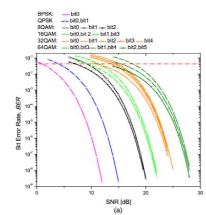
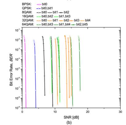
Meanwhile, we apply code rate of 0.7, 0.75, 0.8 to the first and fourth pair, second and fifth pair, and third and sixth pair bit in 64QAM; both configurations will result in the same code rate of 0.75. As shown in Fig. 4, the BER and SNR performance reveals the existence of coding gain improvement of proposed scheme compared with the conventional scheme.
More specifically, the proposed scheme provides 0.5db additional gain at the BER of 10^-15 compared to the corresponding (3-12) , regular QC-LDPC (27708-20781) code when 16 QAM and 64 QAM are used.
Meanwhile, there is no error floor phenomenon observed at BER of 10^-15 after 10^-16 bits have been emulated, which implies the effectiveness of designing the high path QC-LDPC code. It is worth noting that we can further bridge the gap between different bits in large constellation by more flexible component codes , however addressing the difference of latency and the throughput of different component decoder will be very interesting.
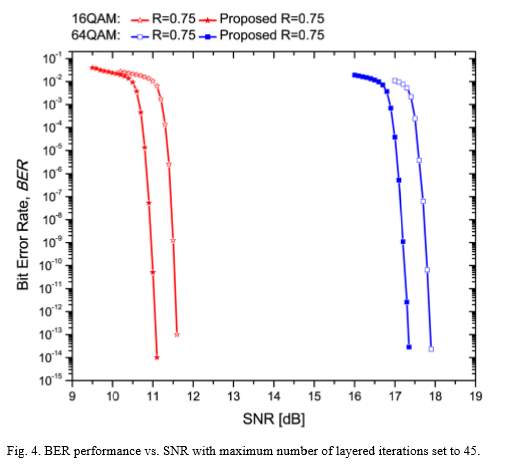
5.6 VNP and CNP Processing
Initialization:
,=0 for =1, =1,…, (2)
Bit decisions:
,= ℎ, +Σ , ′ ′ (3)
̂ ={0, if , ≥01, otherwise (4)
Variable-node update rule:
,= ℎ, +Σ , ′
Note: these (why M terms given means there we used the memory element to represent that we used the equations in following manner)
MESSAGE PASSING THROUGH VNP
MESSAGE PASSING THROUGH CNP
ABS(absolute value and the sign value of the input)
After this find the first and the second minimum values of the absolute values and trace back to find the position of first minimum via binary search tree (BST). It is worth noting that the number of muxes involved in BST and the latency associated with BST are proportional to the number of inputs.
Chapter 6
RESULTS AND DISCUSSION
6.1 Simulation result
Encoded outputusing LDPC codes: 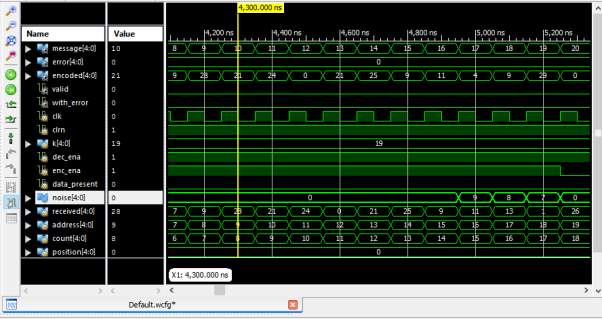
Decoded output using LDPC codes: 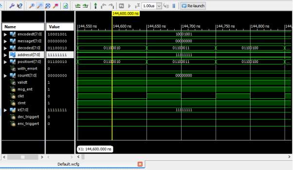
Above shown is the simulation result of the rate compatible LDPC codes. Message is the input data which we have to transmit through the optical fibre for the long distance. Encoded is the coded data of the input message that is to be transmitted. Decoded is the decoded data of the message transmitted. Positions are allocated to the addresses beforehand allocated. Count is the counter which counts the clock seconds. Clkt and clrnt are the inputs given.
6.2 RTL view
RTL is the register transfer logic. RTL view shows the logic circuit for the input code provided. It shows the connections of the logic design. We can verify the functionality of the program by using the RTL view.
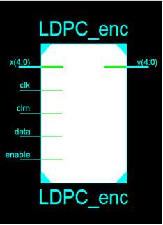
Above shown is the RTL view of the LDPC encoder with input clk, clrn, data, enable and with outputs .Encoder is a combinational circuit consists of 2^n*n inputs and outputs and it also converts the decimal data into encoded form(i.e binary form).
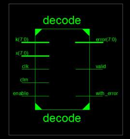
Above shown is the RTL view of the LDPC decoder with input clk, clrn, data, enable and with outputs .Decoder is a combinational circuit consists of n*2^n inputs and outputs and it also converts the encoded data (i.e binary form) into decimal form.
6.3 Timing report
Timing report shows the time taken for the program to be simulated. The time delay for encoding and decoding are shown in the below figures. The time delay for the LDPC encoder is 10.006ns. And for decoding process it is 9.817ns.
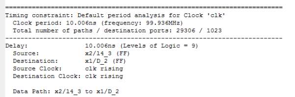
Before implementing the projected RC LDPC codes in hardware, division is a crucial issue that must be addressed. Though a non-uniform division and totally different division strategies are often accustomed represent ,, , and ℎ, ; we have a tendency to use the uniform division theme for all 3 styles of messages. we decide 6-bit resolution to make sure that the error-floor development is attributable to the code-design itself rather than finite preciseness illustration, whereas keeping the complexness moderately low. The FPGA-based emulation was conducted over binary (BI)-AWGN channel, that is valid assumption for associate amplified spontaneous emission (ASE) noise dominated situation.
Given a mother code of girth-10 regular (34635, two7710) created victimization the tactic mentioned in Section 2, a group of RC LDPC codes are often obtained with code rates of by software-based reconfiguration of puncturing-mux and generalized-mux registers in FPGA. With higher than resolution, six RC LDPC decoders are often enforced in one FPGA and with four FPGAs accessible in our fast prototyping platform, in total twenty four decoders area unit utilized.
Each decoder consists of 3 CNPs and 45 VNPs in the implementation, hence the throughput of the decoder can be calculated by ∗ /[( ⁄ + )∗ ] , where = 200 MHz is the FPGA running frequency, is number of bits per codeword, = 2309 is the block size, = 3 is the pipeline depth, = 7 is the latency of VNP and CNP, = 45 is the maximum number of layered iterations. It is worth noting that the decoder will converge fast at high SNR regime (20-27 iterations verified by simulation). The aggregation throughput of the mother code will be ~4.8Gbit/s at low SNR regime and ~9.6Gbit/s at high SNR regime, while the throughput of code rate of 0.6858 will be ~3.2Gbit/s and ~6.4Gbit/s respectively.
The FPGA-based BER vs. Q-factor performance of the projected RC LDPC code is conferred in Fig. 4, within which the parameters within the legend represents the column-weight, row-weight, and therefore the distance of 2 uniformly distributed generalized check-nodes and with variety of stratified iterations set to forty five, that is resembling thirty standard iterations since stratified decipherment converge doubly quicker than standard decipherment formula [18].
It is price mentioning that we tend to puncture the whole block from (3, 15) LDPC mother code for the coarse-tuning and replace each d-th check node with an easy (15, 11) overacting code, wherever ∈ , for the fine-tuning. The mother code with code rate of zero.8 and therefore the lowest code rate of 0.6858 are able to do a letter of the alphabet limit of five.33 decibel and four.2 decibel at BER of 10^-15, which corresponds to the coding gains ranging from 12.67 dB and 13.8 dB.
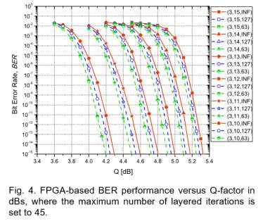
Chapter 7
CONCLUSION AND FUTURE SCOPE
7.1 Conclusion
In this project, we have proposed rate compatible LDPC codes with over head ranging from 25% to 46% for high speed optical transmission systems. The bit error rate performance has been verifies through FPGA emulation system and it has been shown that the proposed rate compatible LDPC codes exhibit a good performance and excellent error floor performance down to BER of 10^-15.
BCH and LDPC codes are designed, analyzed and implemented using FPGA for Error Detection and Correction mechanism in this research work. LDPC codes can be designed using Sum product algorithm or message passing algorithm. In this research work LDPC encoder and decoder is designed using Sum Product Algorithm (SPA). From the results of the first design analysis, it is concluded that the LDPC encoder and Decoder architecture with Sum-product Algorithm has low Area and delay, when compared with all other conventional error correcting algorithms.
To increase the throughput further, various pipelined techniques are applied to LDPC decoder circuit. Pipelined technique and wave pipelined techniques are used in the LDPC decoder block. In this pipelined technique, register unit is included in various stages. But in the wave pipelined technique, register is controlled by one AND gate. Both the techniques are compared with Non-pipelined LDPC decoder. Wave pipelined techniques offer low area than any other techniques. But pipelined technique provides less delay and high throughput than the other two methods.
Then this Efficient LDPC decoder with wave pipelined circuit is applied in OFDM system to reduce the size and hardware complexity of OFDM transmitter and receiver. Conventional OFDM with Convolution encoder and decoder is compared with proposed OFDM with LDPC encoder and decoder circuits.
From the results, it is observed that OFDM with LDPC encoder and decoder consumes less area and delay than the conventional OFDM techniques. The Proposed LDPC encoder and decoder are applied in Wi-Max standard for 4G applications.
7.2 Future scope
A LDPC encoder and decoder will be designed using Modified Sum product algorithm (MSOP) and Modified Message Passing Algorithm (MMPA). This can be applied to MIMO OFDM for wideband communication system. Previously LDPC with sum product algorithm was designed using wave-pipelined technique for high speed data transmission. Further work is to modify the Message Passing algorithm and to apply the same in Multiple Input Multiple Output (MIMO) OFDM. The evaluation of these MIMO OFDM with LDPC codes for 4G application is to be done as a future work.
REFERENCES
[1] R. G. Gallager, Low-Density Parity-Check Codes. Cambridge, MA: MIT Press, 1963.
[2] R. M. Tanner, “A recursive approach to low complexity codes,” IEEE Trans. Inform. Theory, vol. IT-27, no. 5, pp. 533–547, September 1981.
[3] M. G. Luby, M. Mitzenmacher, M. A. Shokrollahi, D. A. Spielman, and V. Stemann, “Practical loss-resilient codes,” in Proc. 30th ACM Symp. on the Theory of Computing, 1998, pp. 249–258.
[4] M. G. Luby, M. Mitzenmacher, M. A. Shokrollahi, and D. A. Spielman, “Improved low-density parity-check codes using irregular graphs,” IEEE Trans. Inform. Theory, vol. 47, no. 2, pp. 585–598, February 2001.
[5] S.-Y. Chung, G. D. Forney, Jr., T. J. Richardson, and R. L. Urbanke, “On the design of low-density parity-check codes within 0.0045 dB of the Shannon limit,” IEEE Commun. Letters, vol. 5, no. 2, pp. 58–60, February 2001.
[6] T. J. Richardson and R. L. Urbanke, “Efficient encoding of low-density parity-check codes,” IEEE Trans. Inform. Theory, vol. 47, no. 2, pp. 638– 656, February 2001.
[7] D. J. C. MacKay, “Good error-correcting codes based on very sparse matrices,” IEEE Trans. Inform. Theory, vol. 45, no. 2, pp. 399–431, March 1999.
[8] S. B. Wicker, Error Control Systems for Digital Communication and Storage. Upper Saddle River, NJ 07458: Prentice Hall, 1995.
[9] S. Lin and D. J. Costello Jr., Error Control Coding, 2nd ed. New Jersey: Prentice Hall, 2004.
[10] F. J. MacWilliams and N. J. A. Sloane, The Theory of Error-Correcting Codes. Amsterdam: North-Holland, 1977.
[11] W. C. Huffman and V. Pless, Fundamentals of Error Correcting Codes. Cambridge University Press, Cambridge UK, 2003.
[12] C. Berrou and A. Glavieux, “Near optimum error correcting coding and decoding: Turbo codes,” IEEE Trans. Commun., vol. 44, no. 10, pp. 1261– 1271, October 1996.
APPENDIX
Data Code:
module msgrom(msgen,data1, addrs);
input [7:0] addrs;
input msgen;
output [7:0] data1;
reg [7:0] data1;
// an arbitrary data source here
always @ (addrs or msgen)
begin
if(msgen)
data1 = addrs + 1;
else
data1 = 1’b0;
end
endmodule
Decoder Block Code:
module decode(x, error,with_error, enable, valid, k,clk, clrn);
input enable, clk, clrn;
input [7:0] x;
//input [7:0] x,t;
input [7:0] k;
output [7:0] error;
wire [7:0] error;
output with_error, valid;
reg with_error, valid;
wire [7:0] s0, s1, s2, s3, s4, s5, s6, s7, s8, s9, s10, s11, s12, s13, s14, s15, s16, s17, s18, s19, s20, s21, s22, s23, s24, s25, s26, s27, s28, s29, s30, s31;
wire [7:0] lambda, omega, alpha;
reg [5:0] count;
reg [32:0] phase;
wire [7:0] D0, D1, DI;
reg [7:0] D, D2;
reg [7:0] u, length0, length1, length2, length3;
reg syn_enable, syn_init, syn_shift, berl_enable;
reg chien_search, chien_load, shorten;
always @ (chien_search or shorten)
valid = chien_search & ~shorten;
olsdec_syn x0 (s0, s1, s2, s3, s4, s5, s6, s7, s8, s9, s10, s11, s12, s13, s14, s15, s16, s17, s18, s19, s20, s21, s22, s23, s24, s25, s26, s27, s28, s29, s30, s31,
u, syn_enable, syn_shift&phase[0], syn_init, clk, clrn);
olsdec x1 (lambda, omega,
s0, s31, s30, s29, s28, s27, s26, s25, s24, s23, s22, s21, s20, s19, s18, s17, s16, s15, s14, s13, s12, s11, s10, s9, s8, s7, s6, s5, s4, s3, s2, s1,
D0, D2, count, phase[0], phase[32], berl_enable, clk, clrn);
error_det2 x2 (error, alpha, lambda, omega,D1,DI, chien_search, chien_load, shorten, clk, clrn);
// error_det2 x2(.error(error), .alpha(alpha), .lambda(lambda), .omega(omega), .even(D1),.D(DI), .search(search), .load(load), .shorten(shorten), .clk(clk), .clrn(clrn));
inverse x3 (DI, D);
always @ (posedge clk or negedge clrn)
begin
if (~clrn)
begin
syn_enable <= 0;
syn_shift <= 0;
berl_enable <= 0;
chien_search <= 1;
chien_load <= 0;
length0 <= 0;
length2 <= 255 – k;
count <= -1;
phase <= 1;
u <= 0;
shorten <= 1;
syn_init <= 0;
end
else
begin
if (enable & ~syn_enable & ~syn_shift)
begin
syn_enable <= 1;
syn_init <= 1;
end
if (syn_enable)
begin
length0 <= length1;
syn_init <= 0;
if (length1 == k)
begin
syn_enable <= 0;
syn_shift <= 1;
berl_enable <= 1;
end
end
if (berl_enable & with_error)
begin
if (phase[0])
begin
count <= count + 1;
if (count == 31)
begin
syn_shift <= 0;
length0 <= 0;
chien_load <= 1;
length2 <= length0;
end
end
phase <= {phase[31:0], phase[32]};
end
if (berl_enable & ~with_error)
if (&count)
begin
syn_shift <= 0;
length0 <= 0;
berl_enable <= 0;
end
else
phase <= {phase[31:0], phase[32]};
if (chien_load & phase[32])
begin
berl_enable <= 0;
chien_load <= 0;
chien_search <= 1;
count <= -1;
phase <= 1;
end
if (chien_search)
begin
length2 <= length3;
if (length3 == 0)
chien_search <= 0;
end
if (enable) u <= x;
if (shorten == 1 && length2 == 0)
shorten <= 0;
end
end
always @ (chien_search or D0 or D1)
if (chien_search) D = D1;
else D = D0;
always @ (DI or alpha or chien_load)
if (chien_load) D2 = alpha;
else D2 = DI;
always @ (length0) length1 = length0 + 1;
always @ (length2) length3 = length2 – 1;
always @ (syn_shift or s0 or s1 or s2 or s3 or s4 or s5 or s6 or s7 or s8 or s9 or s10 or s11 or s12 or s13 or s14 or s15 or s16 or s17 or s18 or s19 or s20 or s21 or s22 or s23 or s24 or s25 or s26 or s27 or s28 or s29 or s30 or s31)
if (syn_shift && (s0 | s1 | s2 | s3 | s4 | s5 | s6 | s7 | s8 | s9 | s10 | s11 | s12 | s13 | s14 | s15 | s16 | s17 | s18 | s19 | s20 | s21 | s22 | s23 | s24 | s25 | s26 | s27 | s28 | s29 | s30 | s31)!= 0)
with_error = 1;
else with_error = 0;
endmodule
Encoder Block Code:
`timescale 1ns / 1ps
/// ENCODER INTERFACE BLOCK ///
module encode (y,x, enable, data, clk, clrn);
input [7:0] x;
input clk, clrn, enable, data;
output [7:0] y;
reg [7:0] y;
wire [7:0] scale0;
wire [7:0] scale1;
wire [7:0] scale2;
wire [7:0] scale3;
wire [7:0] scale4;
wire [7:0] scale5;
wire [7:0] scale6;
wire [7:0] scale7;
wire [7:0] scale8;
wire [7:0] scale9;
wire [7:0] scale10;
wire [7:0] scale11;
wire [7:0] scale12;
wire [7:0] scale13;
wire [7:0] scale14;
wire [7:0] scale15;
wire [7:0] scale16;
wire [7:0] scale17;
wire [7:0] scale18;
wire [7:0] scale19;
wire [7:0] scale20;
wire [7:0] scale21;
wire [7:0] scale22;
wire [7:0] scale23;
wire [7:0] scale24;
wire [7:0] scale25;
wire [7:0] scale26;
wire [7:0] scale27;
wire [7:0] scale28;
wire [7:0] scale29;
wire [7:0] scale30;
wire [7:0] scale31;
reg [7:0] mem0;
reg [7:0] mem1;
reg [7:0] mem2;
reg [7:0] mem3;
reg [7:0] mem4;
reg [7:0] mem5;
reg [7:0] mem6;
reg [7:0] mem7;
reg [7:0] mem8;
reg [7:0] mem9;
reg [7:0] mem10;
reg [7:0] mem11;
reg [7:0] mem12;
reg [7:0] mem13;
reg [7:0] mem14;
reg [7:0] mem15;
reg [7:0] mem16;
reg [7:0] mem17;
reg [7:0] mem18;
reg [7:0] mem19;
reg [7:0] mem20;
reg [7:0] mem21;
reg [7:0] mem22;
reg [7:0] mem23;
reg [7:0] mem24;
reg [7:0] mem25;
reg [7:0] mem26;
reg [7:0] mem27;
reg [7:0] mem28;
reg [7:0] mem29;
reg [7:0] mem30;
reg [7:0] mem31;
reg [7:0] feedback;
ols_enc_m0 m0 (scale0, feedback);
ols_enc_m1 m1 (scale1, feedback);
ols_enc_m2 m2 (scale2, feedback);
ols_enc_m3 m3 (scale3, feedback);
ols_enc_m4 m4 (scale4, feedback);
ols_enc_m5 m5 (scale5, feedback);
ols_enc_m6 m6 (scale6, feedback);
ols_enc_m7 m7 (scale7, feedback);
ols_enc_m8 m8 (scale8, feedback);
ols_enc_m9 m9 (scale9, feedback);
ols_enc_m10 m10 (scale10, feedback);
ols_enc_m11 m11 (scale11, feedback);
ols_enc_m12 m12 (scale12, feedback);
ols_enc_m13 m13 (scale13, feedback);
ols_enc_m14 m14 (scale14, feedback);
ols_enc_m15 m15 (scale15, feedback);
ols_enc_m16 m16 (scale16, feedback);
ols_enc_m17 m17 (scale17, feedback);
ols_enc_m18 m18 (scale18, feedback);
ols_enc_m19 m19 (scale19, feedback);
ols_enc_m20 m20 (scale20, feedback);
ols_enc_m21 m21 (scale21, feedback);
ols_enc_m22 m22 (scale22, feedback);
ols_enc_m23 m23 (scale23, feedback);
ols_enc_m24 m24 (scale24, feedback);
ols_enc_m25 m25 (scale25, feedback);
ols_enc_m26 m26 (scale26, feedback);
ols_enc_m27 m27 (scale27, feedback);
ols_enc_m28 m28 (scale28, feedback);
ols_enc_m29 m29 (scale29, feedback);
ols_enc_m30 m30 (scale30, feedback);
ols_enc_m31 m31 (scale31, feedback);
always @ (posedge clk or negedge clrn)
begin
if (~clrn)//if clear is zero
begin
mem0 <= 0;
mem1 <= 0;
mem2 <= 0;
mem3 <= 0;
mem4 <= 0;
mem5 <= 0;
mem6 <= 0;
mem7 <= 0;
mem8 <= 0;
mem9 <= 0;
mem10 <= 0;
mem11 <= 0;
mem12 <= 0;
mem13 <= 0;
mem14 <= 0;
mem15 <= 0;
mem16 <= 0;
mem17 <= 0;
mem18 <= 0;
mem19 <= 0;
mem20 <= 0;
mem21 <= 0;
mem22 <= 0;
mem23 <= 0;
mem24 <= 0;
mem25 <= 0;
mem26 <= 0;
mem27 <= 0;
mem28 <= 0;
mem29 <= 0;
mem30 <= 0;
mem31 <= 0;
end
else if (enable)// enable is high
begin
mem31 <= mem30 ^ scale31;
mem30 <= mem29 ^ scale30;
mem29 <= mem28 ^ scale29;
mem28 <= mem27 ^ scale28;
mem27 <= mem26 ^ scale27;
mem26 <= mem25 ^ scale26;
mem25 <= mem24 ^ scale25;
mem24 <= mem23 ^ scale24;
mem23 <= mem22 ^ scale23;
mem22 <= mem21 ^ scale22;
mem21 <= mem20 ^ scale21;
mem20 <= mem19 ^ scale20;
mem19 <= mem18 ^ scale19;
mem18 <= mem17 ^ scale18;
mem17 <= mem16 ^ scale17;
mem16 <= mem15 ^ scale16;
mem15 <= mem14 ^ scale15;
mem14 <= mem13 ^ scale14;
mem13 <= mem12 ^ scale13;
mem12 <= mem11 ^ scale12;
mem11 <= mem10 ^ scale11;
mem10 <= mem9 ^ scale10;
mem9 <= mem8 ^ scale9;
mem8 <= mem7 ^ scale8;
mem7 <= mem6 ^ scale7;
mem6 <= mem5 ^ scale6;
mem5 <= mem4 ^ scale5;
mem4 <= mem3 ^ scale4;
mem3 <= mem2 ^ scale3;
mem2 <= mem1 ^ scale2;
mem1 <= mem0 ^ scale1;
mem0 <= scale0;
end
end
always @ (data or x or mem31)
if (data) feedback = x ^ mem31;
else feedback = 0;
always @ (data or x or mem31)
if (data) y = x;
else y = mem31;
endmodule
/// SYNDROME COMPUTATION BLOCKS FOR ENCODER//
module ols_enc_m0 (y, x);
input [7:0] x;
output [7:0] y;
reg [7:0] y;
always @ (x)
begin
y[0] = x[0] ^ x[3] ^ x[5] ^ x[6];
y[1] = x[0] ^ x[1] ^ x[3] ^ x[4] ^ x[5] ^ x[7];
y[2] = x[1] ^ x[2] ^ x[3] ^ x[4];
y[3] = x[0] ^ x[2] ^ x[3] ^ x[4] ^ x[5];
y[4] = x[0] ^ x[1] ^ x[3] ^ x[4] ^ x[5] ^ x[6];
y[5] = x[0] ^ x[1] ^ x[2] ^ x[4] ^ x[5] ^ x[6] ^ x[7];
y[6] = x[1] ^ x[2] ^ x[3] ^ x[5] ^ x[6] ^ x[7];
y[7] = x[2] ^ x[4] ^ x[5] ^ x[7];
end
endmodule
module ols_enc_m1 (y, x);
input [7:0] x;
output [7:0] y;
reg [7:0] y;
always @ (x)
begin
y[0] = x[1] ^ x[2] ^ x[4] ^ x[5];
y[1] = x[0] ^ x[1] ^ x[3] ^ x[4] ^ x[6];
y[2] = x[0] ^ x[7];
y[3] = x[1];
y[4] = x[0] ^ x[2];
y[5] = x[0] ^ x[1] ^ x[3];
y[6] = x[1] ^ x[2] ^ x[4];
y[7] = x[0] ^ x[1] ^ x[3] ^ x[4];
end
endmodule
module ols_enc_m2 (y, x);
input [7:0] x;
output [7:0] y;
reg [7:0] y;
always @ (x)
begin
y[0] = x[0] ^ x[1] ^ x[2] ^ x[3] ^ x[4] ^ x[5];
y[1] = x[0] ^ x[6];
y[2] = x[0] ^ x[2] ^ x[3] ^ x[4] ^ x[5] ^ x[7];
y[3] = x[1] ^ x[3] ^ x[4] ^ x[5] ^ x[6];
y[4] = x[2] ^ x[4] ^ x[5] ^ x[6] ^ x[7];
y[5] = x[3] ^ x[5] ^ x[6] ^ x[7];
y[6] = x[4] ^ x[6] ^ x[7];
y[7] = x[0] ^ x[1] ^ x[2] ^ x[3] ^ x[4] ^ x[7];
end
endmodule
module ols_enc_m3 (y, x);
input [7:0] x;
output [7:0] y;
reg [7:0] y;
always @ (x)
begin
y[0] = x[0] ^ x[2] ^ x[4] ^ x[5] ^ x[7];
y[1] = x[0] ^ x[1] ^ x[2] ^ x[3] ^ x[4] ^ x[6] ^ x[7];
y[2] = x[0] ^ x[1] ^ x[3];
y[3] = x[1] ^ x[2] ^ x[4];
y[4] = x[0] ^ x[2] ^ x[3] ^ x[5];
y[5] = x[0] ^ x[1] ^ x[3] ^ x[4] ^ x[6];
y[6] = x[0] ^ x[1] ^ x[2] ^ x[4] ^ x[5] ^ x[7];
y[7] = x[1] ^ x[3] ^ x[4] ^ x[6] ^ x[7];
end
endmodule
module ols_enc_m4 (y, x);
input [7:0] x;
output [7:0] y;
reg [7:0] y;
always @ (x)
begin
y[0] = x[0] ^ x[1] ^ x[5] ^ x[7];
y[1] = x[2] ^ x[5] ^ x[6] ^ x[7];
y[2] = x[0] ^ x[1] ^ x[3] ^ x[5] ^ x[6];
y[3] = x[0] ^ x[1] ^ x[2] ^ x[4] ^ x[6] ^ x[7];
y[4] = x[1] ^ x[2] ^ x[3] ^ x[5] ^ x[7];
y[5] = x[2] ^ x[3] ^ x[4] ^ x[6];
y[6] = x[0] ^ x[3] ^ x[4] ^ x[5] ^ x[7];
y[7] = x[0] ^ x[4] ^ x[6] ^ x[7];
end
endmodule
module ols_enc_m5 (y, x);
input [7:0] x;
output [7:0] y;
reg [7:0] y;
always @ (x)
begin
y[0] = x[0] ^ x[1] ^ x[4];
y[1] = x[0] ^ x[2] ^ x[4] ^ x[5];
y[2] = x[3] ^ x[4] ^ x[5] ^ x[6];
y[3] = x[0] ^ x[4] ^ x[5] ^ x[6] ^ x[7];
y[4] = x[0] ^ x[1] ^ x[5] ^ x[6] ^ x[7];
y[5] = x[1] ^ x[2] ^ x[6] ^ x[7];
y[6] = x[0] ^ x[2] ^ x[3] ^ x[7];
y[7] = x[0] ^ x[3];
end
endmodule
module ols_enc_m6 (y, x);
input [7:0] x;
output [7:0] y;
reg [7:0] y;
always @ (x)
begin
y[0] = x[0] ^ x[1] ^ x[2] ^ x[4] ^ x[5] ^ x[6] ^ x[7];
y[1] = x[0] ^ x[3] ^ x[4];
y[2] = x[2] ^ x[6] ^ x[7];
y[3] = x[3] ^ x[7];
y[4] = x[0] ^ x[4];
y[5] = x[0] ^ x[1] ^ x[5];
y[6] = x[1] ^ x[2] ^ x[6];
y[7] = x[0] ^ x[1] ^ x[3] ^ x[4] ^ x[5] ^ x[6];
end
endmodule
module ols_enc_m7 (y, x);
input [7:0] x;
output [7:0] y;
reg [7:0] y;
always @ (x)
begin
y[0] = x[0] ^ x[1] ^ x[3] ^ x[5] ^ x[6] ^ x[7];
y[1] = x[0] ^ x[2] ^ x[3] ^ x[4] ^ x[5];
y[2] = x[4] ^ x[7];
y[3] = x[0] ^ x[5];
y[4] = x[0] ^ x[1] ^ x[6];
y[5] = x[0] ^ x[1] ^ x[2] ^ x[7];
y[6] = x[0] ^ x[1] ^ x[2] ^ x[3];
y[7] = x[0] ^ x[2] ^ x[4] ^ x[5] ^ x[6] ^ x[7];
end
endmodule
module ols_enc_m8 (y, x);
input [7:0] x;
output [7:0] y;
reg [7:0] y;
always @ (x)
begin
y[0] = x[0] ^ x[1] ^ x[6];
y[1] = x[2] ^ x[6] ^ x[7];
y[2] = x[0] ^ x[1] ^ x[3] ^ x[6] ^ x[7];
y[3] = x[1] ^ x[2] ^ x[4] ^ x[7];
y[4] = x[2] ^ x[3] ^ x[5];
y[5] = x[3] ^ x[4] ^ x[6];
y[6] = x[0] ^ x[4] ^ x[5] ^ x[7];
y[7] = x[0] ^ x[5];
end
endmodule
module ols_enc_m9 (y, x);
input [7:0] x;
output [7:0] y;
reg [7:0] y;
always @ (x)
begin
y[0] = x[1] ^ x[2] ^ x[5] ^ x[7];
y[1] = x[1] ^ x[3] ^ x[5] ^ x[6] ^ x[7];
y[2] = x[0] ^ x[1] ^ x[4] ^ x[5] ^ x[6];
y[3] = x[0] ^ x[1] ^ x[2] ^ x[5] ^ x[6] ^ x[7];
y[4] = x[1] ^ x[2] ^ x[3] ^ x[6] ^ x[7];
y[5] = x[0] ^ x[2] ^ x[3] ^ x[4] ^ x[7];
y[6] = x[1] ^ x[3] ^ x[4] ^ x[5];
y[7] = x[0] ^ x[1] ^ x[4] ^ x[6] ^ x[7];
end
endmodule
module ols_enc_m10 (y, x);
input [7:0] x;
output [7:0] y;
reg [7:0] y;
always @ (x)
begin
y[0] = x[1] ^ x[3] ^ x[4] ^ x[7];
y[1] = x[1] ^ x[2] ^ x[3] ^ x[5] ^ x[7];
y[2] = x[1] ^ x[2] ^ x[6] ^ x[7];
y[3] = x[0] ^ x[2] ^ x[3] ^ x[7];
y[4] = x[1] ^ x[3] ^ x[4];
y[5] = x[0] ^ x[2] ^ x[4] ^ x[5];
y[6] = x[0] ^ x[1] ^ x[3] ^ x[5] ^ x[6];
y[7] = x[0] ^ x[2] ^ x[3] ^ x[6];
end
endmodule
module ols_enc_m11 (y, x);
input [7:0] x;
output [7:0] y;
reg [7:0] y;
always @ (x)
begin
y[0] = x[2] ^ x[3] ^ x[4] ^ x[6] ^ x[7];
y[1] = x[2] ^ x[5] ^ x[6];
y[2] = x[0] ^ x[2] ^ x[4];
y[3] = x[0] ^ x[1] ^ x[3] ^ x[5];
y[4] = x[1] ^ x[2] ^ x[4] ^ x[6];
y[5] = x[2] ^ x[3] ^ x[5] ^ x[7];
y[6] = x[0] ^ x[3] ^ x[4] ^ x[6];
y[7] = x[1] ^ x[2] ^ x[3] ^ x[5] ^ x[6];
end
endmodule
module ols_enc_m12 (y, x);
input [7:0] x;
output [7:0] y;
reg [7:0] y;
always @ (x)
begin
y[0] = x[1] ^ x[3];
y[1] = x[0] ^ x[1] ^ x[2] ^ x[3] ^ x[4];
y[2] = x[2] ^ x[4] ^ x[5];
y[3] = x[3] ^ x[5] ^ x[6];
y[4] = x[0] ^ x[4] ^ x[6] ^ x[7];
y[5] = x[0] ^ x[1] ^ x[5] ^ x[7];
y[6] = x[0] ^ x[1] ^ x[2] ^ x[6];
y[7] = x[0] ^ x[2] ^ x[7];
end
endmodule
module ols_enc_m13 (y, x);
input [7:0] x;
output [7:0] y;
reg [7:0] y;
always @ (x)
begin
y[0] = x[2] ^ x[3] ^ x[6] ^ x[7];
y[1] = x[2] ^ x[4] ^ x[6];
y[2] = x[0] ^ x[2] ^ x[5] ^ x[6];
y[3] = x[1] ^ x[3] ^ x[6] ^ x[7];
y[4] = x[0] ^ x[2] ^ x[4] ^ x[7];
y[5] = x[1] ^ x[3] ^ x[5];
y[6] = x[0] ^ x[2] ^ x[4] ^ x[6];
y[7] = x[1] ^ x[2] ^ x[5] ^ x[6];
end
endmodule
module ols_enc_m14 (y, x);
input [7:0] x;
output [7:0] y;
reg [7:0] y;
always @ (x)
begin
y[0] = x[0] ^ x[5];
y[1] = x[1] ^ x[5] ^ x[6];
y[2] = x[0] ^ x[2] ^ x[5] ^ x[6] ^ x[7];
y[3] = x[0] ^ x[1] ^ x[3] ^ x[6] ^ x[7];
y[4] = x[1] ^ x[2] ^ x[4] ^ x[7];
y[5] = x[2] ^ x[3] ^ x[5];
y[6] = x[3] ^ x[4] ^ x[6];
y[7] = x[4] ^ x[7];
end
endmodule
module ols_enc_m15 (y, x);
input [7:0] x;
output [7:0] y;
reg [7:0] y;
always @ (x)
begin
y[0] = x[0] ^ x[1] ^ x[2] ^ x[3] ^ x[4] ^ x[5] ^ x[7];
y[1] = x[6] ^ x[7];
y[2] = x[0] ^ x[1] ^ x[2] ^ x[3] ^ x[4] ^ x[5];
y[3] = x[1] ^ x[2] ^ x[3] ^ x[4] ^ x[5] ^ x[6];
y[4] = x[2] ^ x[3] ^ x[4] ^ x[5] ^ x[6] ^ x[7];
y[5] = x[3] ^ x[4] ^ x[5] ^ x[6] ^ x[7];
y[6] = x[4] ^ x[5] ^ x[6] ^ x[7];
y[7] = x[0] ^ x[1] ^ x[2] ^ x[3] ^ x[4] ^ x[6];
end
endmodule
Cite This Work
To export a reference to this article please select a referencing stye below:
Related Services
View all


Related Content
All TagsContent relating to: "Technology"
Technology can be described as the use of scientific and advanced knowledge to meet the requirements of humans. Technology is continuously developing, and is used in almost all aspects of life.
Related Articles

DMCA / Removal Request
If you are the original writer of this dissertation and no longer wish to have your work published on the UKDiss.com website then please: